|
|
|
PDF NDH834P Data sheet ( Hoja de datos )
| Número de pieza | NDH834P | |
| Descripción | P-Channel Enhancement Mode Field Effect Transistor | |
| Fabricantes | Fairchild | |
| Logotipo | ||
Hay una vista previa y un enlace de descarga de NDH834P (archivo pdf) en la parte inferior de esta página. Total 8 Páginas | ||
|
No Preview Available !
May 1997
NDH834P
P-Channel Enhancement Mode Field Effect Transistor
General Description
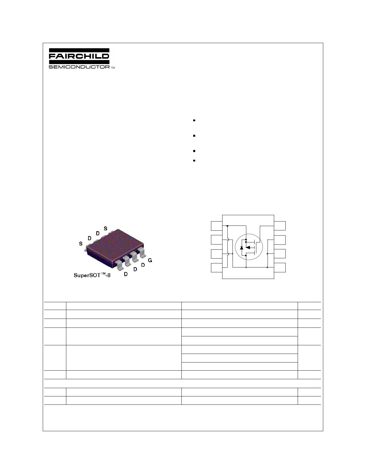
SuperSOTTM-8 P-Channel enhancement mode power field
effect transistors are produced using Fairchild's proprietary,
high cell density, DMOS technology. This very high density
process is especially tailored to minimize on-state resistance
and provide superior switching performance. These devices
are particularly suited for low voltage applications such as
battery powered circuits or portable electronics where fast
switching, low in-line power loss, and resistance to transients
are needed.
Features
-5.6 A, -20 V. RDS(ON) = 0.035 Ω @ VGS = -4.5 V
RDS(ON) = 0.045 Ω @ VGS = -2.7V.
Proprietary SuperSOTTM-8 package design using copper
lead frame for superior thermal and electrical capabilities.
High density cell design for extremely low RDS(ON).
Exceptional on-resistance and maximum DC current
capability.
____________________________________________________________________________________________
54
63
72
81
Absolute Maximum Ratings TA = 25°C unless otherwise noted
Symbol Parameter
VDSS Drain-Source Voltage
VGSS Gate-Source Voltage
ID Drain Current - Continuous
- Pulsed
(Note 1a)
PD Maximum Power Dissipation
(Note 1a)
(Note 1b)
(Note 1c)
TJ,TSTG Operating and Storage Temperature Range
THERMAL CHARACTERISTICS
RqJA
RqJC
Thermal Resistance, Junction-to-Ambient
Thermal Resistance, Junction-to-Case
(Note 1a)
(Note 1)
NDH834P
-20
±8
-5.6
-15
1.8
1
0.9
-55 to 150
70
20
Units
V
V
A
W
°C
°C/W
°C/W
© 1997 Fairchild Semiconductor Corporation
NDH834P Rev.C
1 page 
Typical Electrical Characteristics
1.1
1.08
1.06
I = -250µA
D
1.04
1.02
1
0.98
0.96
0.94
0.92
-50
-25
0 25 50 75 100 125 150
T J , JUNCTION TEMPERATURE (°C)
Figure 7. Breakdown Voltage Variation
with Temperature.
5000
3000
2000
1000
Ciss
Coss
500
300 f = 1 MHz
VGS = 0 V
Crss
150
0 .1
0 .2
0 .5 1
2
5 10
-VDS , DRAIN TO SOURCE VOLTAGE (V)
20 30
Figure 9. Capacitance Characteristics.
15
5 VGS = 0V
1
0 .1
0 .0 1
TJ = 125°C
25°C
-55°C
0 .0 0 1
0 .0 0 0 1
0
0 .2 0 .4 0.6 0 .8
1
-VSD , BODY DIODE FORWARD VOLTAGE (V)
Figure 8. Body Diode Forward Voltage
Variation with Current and
Temperature.
1 .2
5
I = -5.6A
D
4
3
VDS = -5V
-10V
-15V
2
1
0
02468
Q , GATE CHARGE (nC)
g
Figure 10. Gate Charge Characteristics.
10
VIN
VG S
RGEN
G
-VD D
RL
D
VOUT
DUT
S
t d(on)
ton
tr
90%
td(off)
toff
tf
90%
VO U T
VIN
10%
10%
50%
10%
90%
50%
PULSE WIDTH
INVERTED
Figure 11. Switching Test Circuit.
Figure 12. Switching Waveforms.
NDH834P Rev.C
5 Page | ||
| Páginas | Total 8 Páginas | |
| PDF Descargar | [ Datasheet NDH834P.PDF ] | |
Hoja de datos destacado
| Número de pieza | Descripción | Fabricantes |
| NDH834P | P-Channel Enhancement Mode Field Effect Transistor | Fairchild |
| Número de pieza | Descripción | Fabricantes |
| SLA6805M | High Voltage 3 phase Motor Driver IC. |
Sanken |
| SDC1742 | 12- and 14-Bit Hybrid Synchro / Resolver-to-Digital Converters. |
Analog Devices |
|
DataSheet.es es una pagina web que funciona como un repositorio de manuales o hoja de datos de muchos de los productos más populares, |
| DataSheet.es | 2020 | Privacy Policy | Contacto | Buscar |