|
|
|
PDF NJW4191 Data sheet ( Hoja de datos )
| Número de pieza | NJW4191 | |
| Descripción | Inverting Charge Pump IC | |
| Fabricantes | New Japan Radio | |
| Logotipo | ||
Hay una vista previa y un enlace de descarga de NJW4191 (archivo pdf) en la parte inferior de esta página. Total 7 Páginas | ||
|
No Preview Available !
Inverting Charge Pump IC
NJW4191
GENERAL DESCRIPTION
The NJW4191 is the inverting charge pump IC that operates
wide 4.7V to 17V input range. With only the external part of an
input/output capacitor and a charge pump capacitor, can compose
the inverting voltage circuit. It has a high current capability and a
corresponding to small-sized capacitor compared with conventional
product such as popular 7660/7662.
For usability, it has ON/OFF function, Output Voltage Adjustable
function and external synchronous function.
The NJW4191 is suitable for the bias voltage of a liquid crystal
panels, CCD, sensors and operational amplifiers.
There is the NJW4190 for doubler voltage output application.
PACKAGE OUTLINE
NJW4191R
NJW4191M
FEATURES
Inverted Output
-17V max.
Wide Operating Voltage Range
4.7V to 17V
Maximum Output Current
55mA max.
Correspond to Ceramic Capacitor (MLCC)
VOUT Programmable
ON/OFF Function
http://www.DataSheet4U.net/
Built-in Oscillation Circuit
300kHz typ.
External Synchronization Function divide-by-4 counter (A ver.)
Thermal Shutdown
Function Compatible to NJU7660/NJU7662 Inverting Circuit*
Package Outline
NJW4191R
: MSOP8 (VSP8)**
NJW4191M
: DMP8
* The NJW4191 is not pin compatible to NJU7660/62.
** MEET JEDEC MO-187-DA
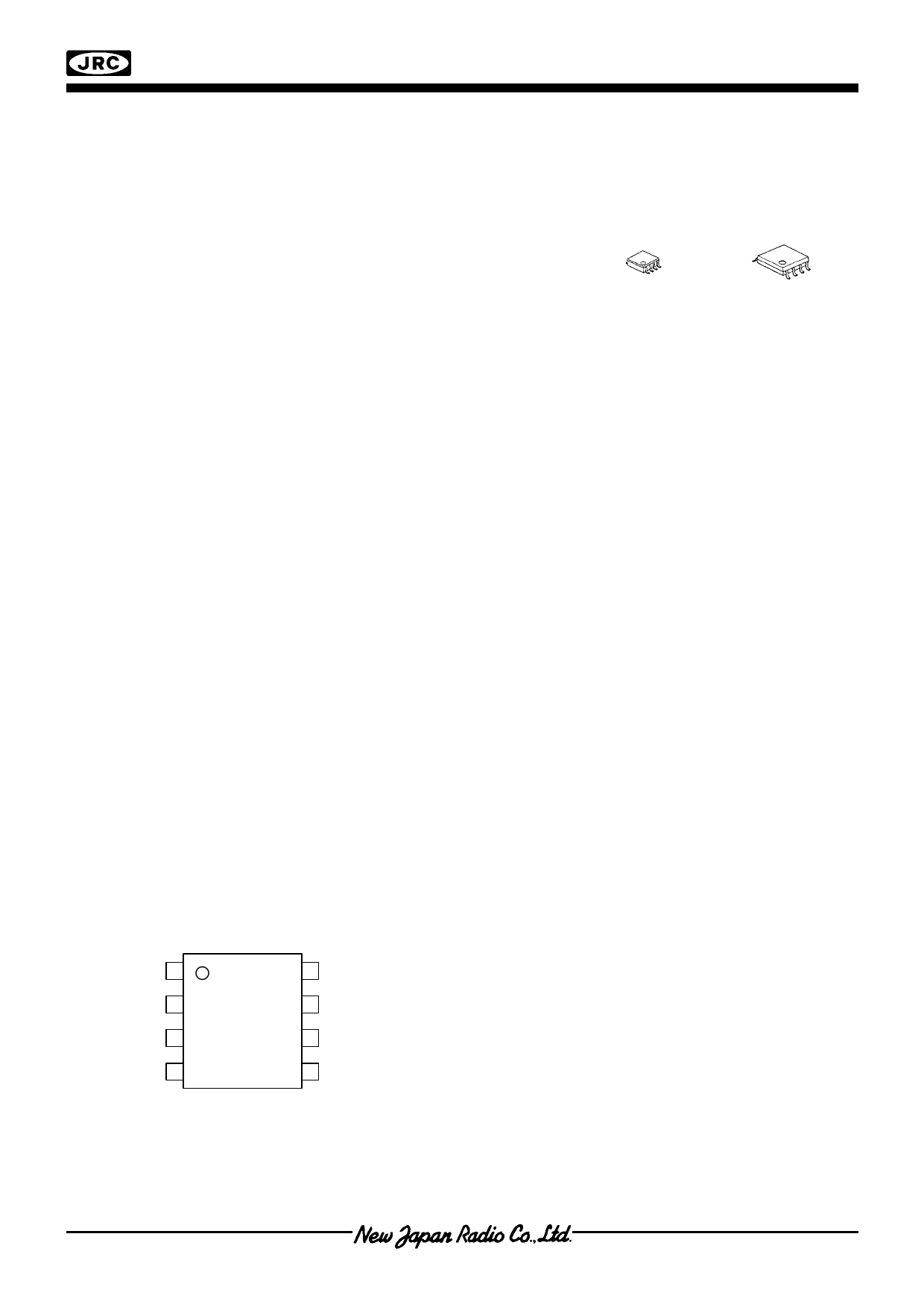
PIN CONFIGURATION
1
2
3
4
NJW4191R
NJW4191M
PIN FUNCTION
8 1. FB
7
2. C+
3. GND
6 4. C-
5. VOUT
5 6. ON/OFF
7. CLK
8. V+
Ver.2013-02-12
-1-
datasheet pdf - http://www.DataSheet4U.net/
1 page 
NJW4191
CHARACTERISTICS
Power Efficiency vs. Output Current
(V+=10V, C1=C2=C3=1µF, Ta=25oC)
100
90
80
70
60
50
40
30
20
10
0
0 10 20 30 40 50 60
Output Current I (mA)
OUT
Output voltage vs. Output Current
(V+=10V, C1=C2=C3=1µF, Ta=25oC)
0
-2
-4
-6
-8
-10
0
10 20 30 40 50
Output Current I (mA)
OUT
60
Output Resistance vs. Temperature
(V+=10V, C1=C2=C3=1µF, I =20mA)
50 OUT
40
30
20
10
0
-50 -25 0 25 50 75 100 125 150
Ambient Temperature Ta (oC)
Oscillation Frequency vs. Temperature
(V+=10V, C1=C2=C3=1µF)
360
340
320
http://www.DataSheet4U.net/
300
280
260
240
-50 -25 0 25 50 75 100 125 150
Ambient Temperature Ta (oC)
FB Detection Voltage vs. Temperature
1.4 (V+=10V, C1=C2=C3=1µF)
1.35
1.3
1.25
1.2
1.15
-50 -25 0 25 50 75 100 125 150
Ambient Temperature Ta (oC)
Ver.2013-02-12
-5-
datasheet pdf - http://www.DataSheet4U.net/
5 Page | ||
| Páginas | Total 7 Páginas | |
| PDF Descargar | [ Datasheet NJW4191.PDF ] | |
Hoja de datos destacado
| Número de pieza | Descripción | Fabricantes |
| NJW4190 | Doubler Charge Pump IC | New Japan Radio |
| NJW4191 | Inverting Charge Pump IC | New Japan Radio |
| NJW4196 | Internal 3.5A MOSFET Switching Regulator IC | New Japan Radio |
| Número de pieza | Descripción | Fabricantes |
| SLA6805M | High Voltage 3 phase Motor Driver IC. |
Sanken |
| SDC1742 | 12- and 14-Bit Hybrid Synchro / Resolver-to-Digital Converters. |
Analog Devices |
|
DataSheet.es es una pagina web que funciona como un repositorio de manuales o hoja de datos de muchos de los productos más populares, |
| DataSheet.es | 2020 | Privacy Policy | Contacto | Buscar |