|
|
|
PDF HI-1566 Data sheet ( Hoja de datos )
| Número de pieza | HI-1566 | |
| Descripción | (HI-1565 / HI-1566) 5V Monolithic Dual Transceivers | |
| Fabricantes | HOLTIC | |
| Logotipo | ||
Hay una vista previa y un enlace de descarga de HI-1566 (archivo pdf) en la parte inferior de esta página. Total 9 Páginas | ||
|
No Preview Available !
August 2006
HI-1565, HI-1566
MIL-STD-1553 / 1760
5V Monolithic Dual Transceivers
DESCRIPTION
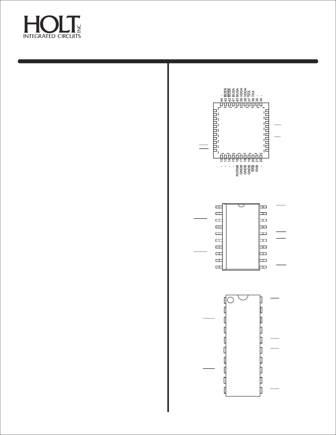
PIN CONFIGURATIONS
The HI-1565 and HI-1566 are low power CMOS dual
transceivers designed to meet the requirements of the
MIL-STD-1553 /1760 specifications.
The transmitter section of each channel takes
complementary CMOS / TTL digital input data and
converts it to bi-phase Manchester encoded 1553 signals
suitable for driving the bus isolation transformer. Separate
transmitter inhibit control signals are provided for each
transmitter.
The receiver section of each channel converts the 1553
bus bi-phase data to complementary CMOS / TTL data
suitable for inputting to a Manchester decoder. Each
receiver has a separate enable input which can be used to
force the output of the receiver to a logic 0 (HI-1565) or
logic 1 (HI-1566).
To minimize the package size for this function, the
transmitter outputs are internally connected to the receiver
inputs, so that only two pins are required for connection to
eachwww.DataSheet4U.com coupling transformer.
FEATURES
! Compliant to MIL-STD-1553A & B,
MIL-STD-1760, ARINC 708A
! CMOS technology for low standby power
! Smallest footprint available in 44-pin plastic
chip-scale package with integral heatsink
! Less than 1.0W maximum power dissipation
! BUS pins ESD protected to greater than 8KV
! Also available in DIP and small outline
(ESOIC) package options
! Military processing options
! Industry standard pin configurations
-1
RXENA 2
GNDA 3
GNDA 4
GNDA 5
VDDB 6
VDDB 7
BUSB 8
BUSB 9
BUSB 10
BUSB 11
1565PCI
1565PCT
1566PCI
1566PCT
33 -
32 -
31 TXINHA
30 RXA
29 RXA
28 -
27 -
26 TXB
25 TXB
24 TXINHB
23 -
44 Pin Plastic 7mm x 7mm
Chip-scale package
VDDA 1
BUSA 2
BUSA 3
RXENA 4
GNDA 5
VDDB 6
BUSB 7
BUSB 8
RXENB 9
GNDB 10
1565PSI
1565PST
1565PSM
1565PSI
1565PST
1565PSM
20 TXA
19 TXA
18 TXINHA
17 RXA
16 RXA
15 TXB
14 TXB
13 TXINHB
12 RXB
11 RXB
20 Pin Plastic ESOIC - WB package
VDDA 1
BUSA 2
BUSA 3
RXENA 4
GNDA 5
VDDB 6
BUSB 7
BUSB 8
RXENB 9
GNDB 10
1565CDI
1565CDT
1565CDM
1566CDI
1566CDT
1566CDM
20 TXA
19 TXA
18 TXINHA
17 RXA
16 RXA
15 TXB
14 TXB
13 TXINHB
12 RXB
11 RXB
20 Pin Ceramic DIP package
(DS1565 Rev. A)
HOLT INTEGRATED CIRCUITS
www.holtic.com
08/06
1 page 
HI-1565, HI-1566
DC ELECTRICAL CHARACTERISTICS (cont.)
VDD = 5.0V, GND = 0V, TA = Operating Temperature Range (unless otherwise specified).
PARAMETER
SYMBOL
CONDITION
TRANSMITTER (Measured at Point “AD” in Figure 2 unless otherwise specified)
Output Voltage
Direct coupled
Transformer coupled
VOUT
VOUT
35 ohm load
(Measured at Point “AD“ in Figure 2)
70 ohm load
(Measured at Point “AT“ in Figure 3)
Output Noise
VON Differential, inhibited
Output Dynamic Offset Voltage Direct coupled
Transformer coupled
VDYN
VDYN
35 ohm load
(Measured at Point “AD“ in Figure 2)
70 ohm load
(Measured at Point “AT“ in Figure 3)
Output resistance
ROUT
Differential, not transmitting
Output Capacitance
COUT
1 MHz sine wave
MIN
7.0
20.0
-90
-250
10
TYP
MAX UNITS
9.0
27.0
10.0
90
250
15
Vp-p
Vp-p
mVp-p
mV
mV
Kohm
pF
AC ELECTRICAL CHARACTERISTICS
VDD = 5.0V, GND = 0V, TA =Operating Temperature Range (unless otherwise specified).
PARAMETER
SYMBOL TEST CONDITIONS
RECEIVER
(Measured at Point “AD” in Figure 2)
Receiver Delay
tDR From input zero crossing to RXA/B or RXA/B
Receiver gap time
tRG Spacing between RXA/B and RXA/B pulses
Receiver Enable Delay
tREN
From RXENA/B rising or falling edge to
RXA/B or RXA/B
TRANSMITTER (Measured at Point “AD” in Figure 2)
Driver Delay
tDT TXA/B, TXA/B to BUSA/B, BUSA/B
Rise time
tr 35 ohm load
Fall Time
tf 35 ohm load
Inhibit Delay
tDI-H
Inhibited output
tDI-L
Active output
MIN
90
100
100
TYP
MAX UNITS
450 ns
365 ns
40 ns
150 ns
300 ns
300 ns
100 ns
150 ns
TXA/B
TXA/B
TXINHA/B
Point “AD“
TRANSMITTER
BUSA/B
BUSA/B
1:2.5
55 W
Isolation
55 W
Transformer
35 W
55 W
2.5:1
RECEIVER
35 W
55 W
Isolation
Transformer
RXENA/B
Point “AD“
RXA/B
RXA/B
Figure 2. Direct Coupled Test Circuits
HOLT INTEGRATED CIRCUITS
5
5 Page | ||
| Páginas | Total 9 Páginas | |
| PDF Descargar | [ Datasheet HI-1566.PDF ] | |
Hoja de datos destacado
| Número de pieza | Descripción | Fabricantes |
| HI-1565 | (HI-1565 / HI-1566) 5V Monolithic Dual Transceivers | HOLTIC |
| HI-1566 | (HI-1565 / HI-1566) 5V Monolithic Dual Transceivers | HOLTIC |
| HI-1567 | 5V Monolithic Dual Transceivers | HOLTIC |
| HI-1568 | 5V Monolithic Dual Transceivers | HOLTIC |
| Número de pieza | Descripción | Fabricantes |
| SLA6805M | High Voltage 3 phase Motor Driver IC. |
Sanken |
| SDC1742 | 12- and 14-Bit Hybrid Synchro / Resolver-to-Digital Converters. |
Analog Devices |
|
DataSheet.es es una pagina web que funciona como un repositorio de manuales o hoja de datos de muchos de los productos más populares, |
| DataSheet.es | 2020 | Privacy Policy | Contacto | Buscar |