|
|
|
PDF 33390 Data sheet ( Hoja de datos )
| Número de pieza | 33390 | |
| Descripción | Class B Serial Transceiver | |
| Fabricantes | Motorola Inc | |
| Logotipo | ||
Hay una vista previa y un enlace de descarga de 33390 (archivo pdf) en la parte inferior de esta página. Total 16 Páginas | ||
|
No Preview Available !
Freescale Semiconductor, Inc.
MOTOROLA
SEMICONDUCTOR TECHNICAL DATA
Document order number: MC33390/D
Rev 4.0, 2/2003
Class B Serial Transceiver
The 33390 is a serial transceiver designed to provide bi-directional half-
duplex communication meeting the automotive SAE Standard J-1850 Class B
Data Communication Network Interface specification. It is designed to
interface directly to on-board vehicle microcontrollers and serves to transmit
and receive data on a single-wire bus at data rates of 10.4 kbps using Variable
Pulse Width Modulation (VPWM). The 33390 operates directly from a vehicle's
12 V battery system and functions in a logic fashion as an I/O interface
between the microcontroller's 5.0 V CMOS logic level swings and the required
0 V to 7.0 V waveshaped signal swings of the bus. The bus output driver is
short circuit current limited.
Features
• Designed for SAE J-1850 Class B Data Rates
• Full Operational Bus Dynamics Over a Supply Voltage of 9.0 to 16 V
• Ambient Operating Temperature of -40°C to 125°C
• Interfaces Directly to Standard 5.0 V CMOS Microcontroller
• BUS Pin Protected Against Shorts to Battery and Ground
• Thermal Shutdown with Hysteresis
• Voltage Waveshaping of Bus Output Driver
• 40 V Max VBAT Capability
33390
J-1850 SERIAL TRANSCEIVER
D SUFFIX
PLASTIC PACKAGE
CASE 751
(8-LEAD SOICN)
ORDERING INFORMATION
Device
Temperature
Range (TA)
Package
MC33390D/DR2 -40 to 125°C
8 SOICN
© Motorola, Inc. 2003
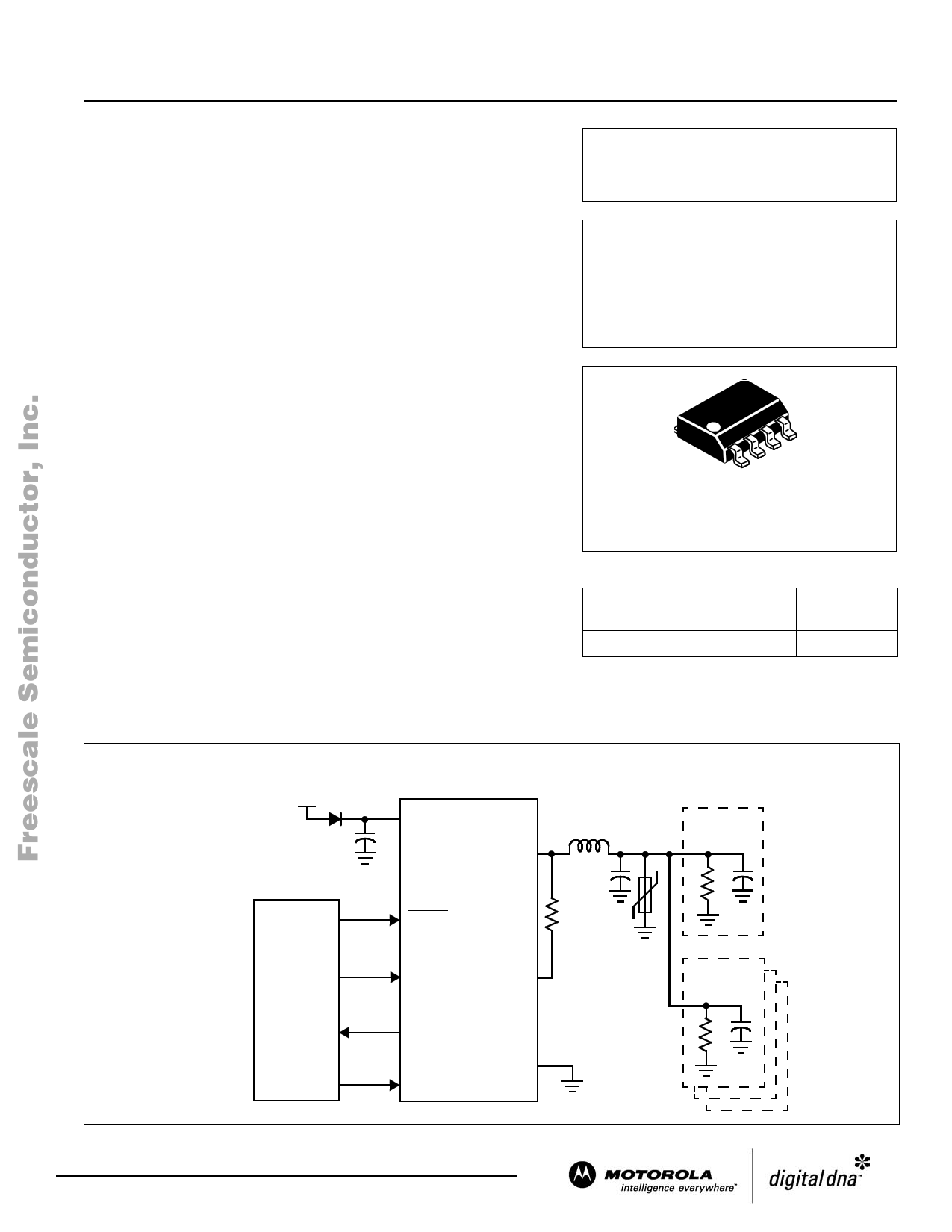
VBAT
33390 Simplified Application Diagram
33390
VBAT
BUS
47 µH
470 pF
SLEEP
10.6 kΩ
MCU
Tx LOAD
Rx
4X/LOOP
GND
Primary
Node
Secondary
Nodes
For More Information On This Product,
Go to: www.freescale.com
1 page 
Freescale Semiconductor, Inc.
STATIC ELECTRICAL CHARACTERISTICS
Characteristics noted under conditions of 7.0 V ≤ VBAT ≤ 16 V, -40°C ≤ TA ≤ 125°C, SLEEP = 5.0 V unless otherwise noted. Typical
values reflect the parameter's approximate midpoint average value with VBAT = 13 V, TA = 25°C. All positive currents are into the
pin. All negative currents are out of the pin.
Characteristic
POWER CONSUMPTION
Symbol Min Typ Max Unit
Operational Battery Current (RMS with Tx = 7.812 kHz Square Wave)
BUS Load = 1380 Ω to GND, 3.6 nF to GND
BUS Load = 257 Ω to GND, 20.2 nF to GND
Battery Bus Low Input Current
After SLEEP Toggle Low to High; Prior to Tx Toggling
After Tx Toggle High to Low
Sleep State Battery Current
VSLEEP = 0 V
BUS
IBAT (OP1)
IBAT (OP2)
IBAT(BUS L1)
IBAT(BUS L2)
IBAT(SLEEP)
–
–
–
–
–
3.0
22.4
1.1
6.4
38.2
mA
11.5
32
mA
3.0
8.5
µA
65
BUS Input Receiver Threshold (Note 5)
Threshold High (Bus Increasing until Rx ≥ 3.0 V)
Threshold Low (Bus Decreasing until Rx ≤ 3.0 V)
Threshold in Sleep State (SLEEP = 0 V)
Hysteresis (VBUS(IH) - VBUS(IL), SLEEP = 0 V)
BUS-Out Voltage (257 Ω ≤ RBUS(L) to GND ≤ 1380 Ω)
8.2 V ≤ VBAT ≤ 16 V, Tx = 5.0 V
4.25 V ≤ VBAT ≤ 8.2 V, Tx = 5.0 V
Tx = 0 V
VBUS(IH)
VBUS(IL)
BUSTH(SLEEP)
VBUS(HYST)
4.25
–
2.4
0.1
VBUS (OUT1)
VBUS (OUT2)
VBUS (OUT3)
6.25
VBAT - 1.6
–
3.9
3.7
3.0
0.2
6.9
–
0.27
–
3.5
3.4
0.6
8.0
VBAT
0.7
V
V
BUS Short Circuit Output Current
Tx = 5.0 V, -2.0 V ≤ VBUS ≤ 4.8 V
BUS Leakage Current
-2.0 V ≤ VBUS ≤ 0 V
0 V ≤ VBUS ≤ VBAT
BUS Thermal Shutdown (Note 6) (Tx = 5.0 V, IBUS = -0.1 mA)
Increase Temperature until VBUS ≤ 2.5 V
BUS Thermal Shutdown Hysteresis (Note 7)
TBUS(LIM) - TBUS(REEN)
BUS and LOAD Current with Loss of VBAT or GND (IBAT = 0 µA) (see Figure 2)
-18 V ≤ VBUS ≤ 9.0 V
-18 V ≤ VLOAD ≤ 9.0 V
IBUS (SHORT)
IBUS (LEAK1)
IBUS (LEAK2)
TBUS (LIM)
TBUS (LI MHYS)
IBUS (LOSS)
ILOAD (LOSS)
60
-500
–
150
10
–
–
129
-55
189
170
12
0.00
0.00
mA
170
µA
–
500
°C
190
°C
15
mA
0.1
0.1
Notes
5. Typical threshold value is the approximate actual occurring switch point value with VBAT = 13 V, TA = 25°C.
6. Device characterized but not production tested for thermal shutdown.
7. Device characterized but not production tested for thermal shutdown hysteresis.
MOTOROLA ANALOG INTEGRATED CIRFCoUIrTMDEoVrICeEIDnAfoTArmation On This Product,
Go to: www.freescale.com
33390
5
5 Page 
Freescale Semiconductor, Inc.
Receiver Protocol
The Class B communication scheme uses a variable pulse
width (VPW) protocol. The microcontroller provides the VPW
decoding function. Once the receiver detects a transition on Rx,
it starts an internal counter. The initial “start of frame” bit is a
logic [1] and lasts 200 µs. For subsequent bits, if there is a bus
transition before 96 µs, one logic state is inferred. If there is a
bus transition after 96 µs, the other logic state is inferred. The
“end of data” bit is a logic [0] and lasts 200 µs. If there is no
activity on the bus for 280 µs to 320 µs following a broadcast
message, multiple unit nodes may arbitrate for control of the
next message. During an arbitration, after the “start of frame” bit
has been transmitted, the secondary node transmitting the
most consecutive logic [0] bits will be granted sole transmission
access to the bus for that message.
Loss of Assembly Ground Connection
The definition of a loss of assembly ground condition at the
device level is that all pins of the 33390, with the exception of
BUS and LOAD, see a very low impedance to VBAT.
The LOAD pin of the device has an internal transistor switch
connected to it that is normally saturated to ground. This pulls
the LOAD-side of the external resistor (tied from BUS to LOAD)
to ground under normal conditions. The LOAD pin switch is
essentially that of an “upside down” FET, which is normally
biased “on” so long as module ground is present and biased
“off” when loss-of-ground occurs. When a loss of assembly
ground occurs, the load transistor switch is self-biased “off”,
allowing no more than 100 µA of leakage current to flow in the
LOAD pin. During such a loss of assembly ground condition, the
BUS and LOAD pins exhibit a high impedance to VBAT; all other
pins will exhibit a low impedance to VBAT. During this condition
the BUS pin is prevented from sourcing any current or loading
the bus, which would cause a corruption of any data being
transmitted on the bus. While a particular assembly is
experiencing a loss of ground, all other assembly nodes are
permitted to function normally. It should be noted that with other
nodes existing on the bus, the bus will always have some
minimum/maximum impedance to ground as shown in Table 1,
page 10.
Loss of Assembly Battery Connection
The definition of a loss of assembly battery condition at the
device level is that the VBAT pin of the 33390 sees an infinite
impedance to VBAT, but there is some undefined impedance
between these pins and ground.
MOTOROLA ANALOG INTEGRATED CIRFCoUIrTMDEoVrICeEIDnAfoTArmation On This Product,
Go to: www.freescale.com
33390
11
11 Page | ||
| Páginas | Total 16 Páginas | |
| PDF Descargar | [ Datasheet 33390.PDF ] | |
Hoja de datos destacado
| Número de pieza | Descripción | Fabricantes |
| 33390 | Class B Serial Transceiver | Motorola Inc |
| 33394 | Switch Mode Power Supply | Freescale Semiconductor |
| 33395 | Three-Phase Gate Driver IC | Freescale Semiconductor |
| 33395T | Three-Phase Gate Driver IC | Freescale Semiconductor |
| Número de pieza | Descripción | Fabricantes |
| SLA6805M | High Voltage 3 phase Motor Driver IC. |
Sanken |
| SDC1742 | 12- and 14-Bit Hybrid Synchro / Resolver-to-Digital Converters. |
Analog Devices |
|
DataSheet.es es una pagina web que funciona como un repositorio de manuales o hoja de datos de muchos de los productos más populares, |
| DataSheet.es | 2020 | Privacy Policy | Contacto | Buscar |