|
|
|
PDF A8293 Data sheet ( Hoja de datos )
| Número de pieza | A8293 | |
| Descripción | Single LNB Supply and Control Voltage Regulator | |
| Fabricantes | Allegro MicroSystems | |
| Logotipo | ||
Hay una vista previa y un enlace de descarga de A8293 (archivo pdf) en la parte inferior de esta página. Total 19 Páginas | ||
|
No Preview Available !
A8293
Single LNB Supply and Control Voltage Regulator
Features and Benefits
Description
▪ 2-wire serial 2IC™ -compatible interface: control (write) and Intended for analog and digital satellite receivers, this single
status (read)
low noise block converter regulator (LNBR) is a monolithic
▪ LNB voltages (8 programmable levels) compatible with
linear and switching voltage regulato,rspecifically designed to
all common standards including domestic Japan models
provide the power and the interface signals to an LNB down
▪ Tracking switch-mode power converter for lowest dissipation converter via coaxial cable. The A8293 requires few external
▪ Integrated converter switches and current sensing
components, with the boost switch and compensation circuitry
▪ Provides up to 700 mA load current
integrated inside of the device.A high switching frequency is
▪ Static current limit circuit allows full current at startup and chosen to minimize the size of the passive filtering components,
13→18V output transition; reliably starts wide load range further assisting in cost reductionT. he high levels of component
▪ Push-pull output stage minimizes 13→18V and 18→13 V integration ensure extremely low noise and ripple figures.
output transition times for highly capacitive loads
▪ Adjustable rise/fall time via external timing capacitor
▪ Built-in tone oscillator, factory-trimmed to 22 kHz
facilitates DiSEqC™ tone encoding, even at no-load
▪ Four methods of 22 kHz tone generation, via I2C™ data
bits and/or external pin
The A8293 has been designed for high ef ficiency, utilizing
the Allegro® advanced BCD process. The integrated boost
switch has been optimized to minimize both switching and
static losses. To further enhance ef ficiency, the voltage drop
across the tracking regulator has been minimized.
▪ Auxiliary modulation input
For DiSEqC™ communications, several schemes are available
▪ LNB overcurrent with timer
for generating tone signals, all the way down to no-load, and
▪ Diagnostics for output voltage level, input supply UVLO using either the internal clock or an external time source.
Packages:
20-contact, 4 × 4 mm
MLP/QFN (suffix ES)
28 contact, 5 × 5 mm
MLP/QFN (suffix ET)
Continued on the next page…
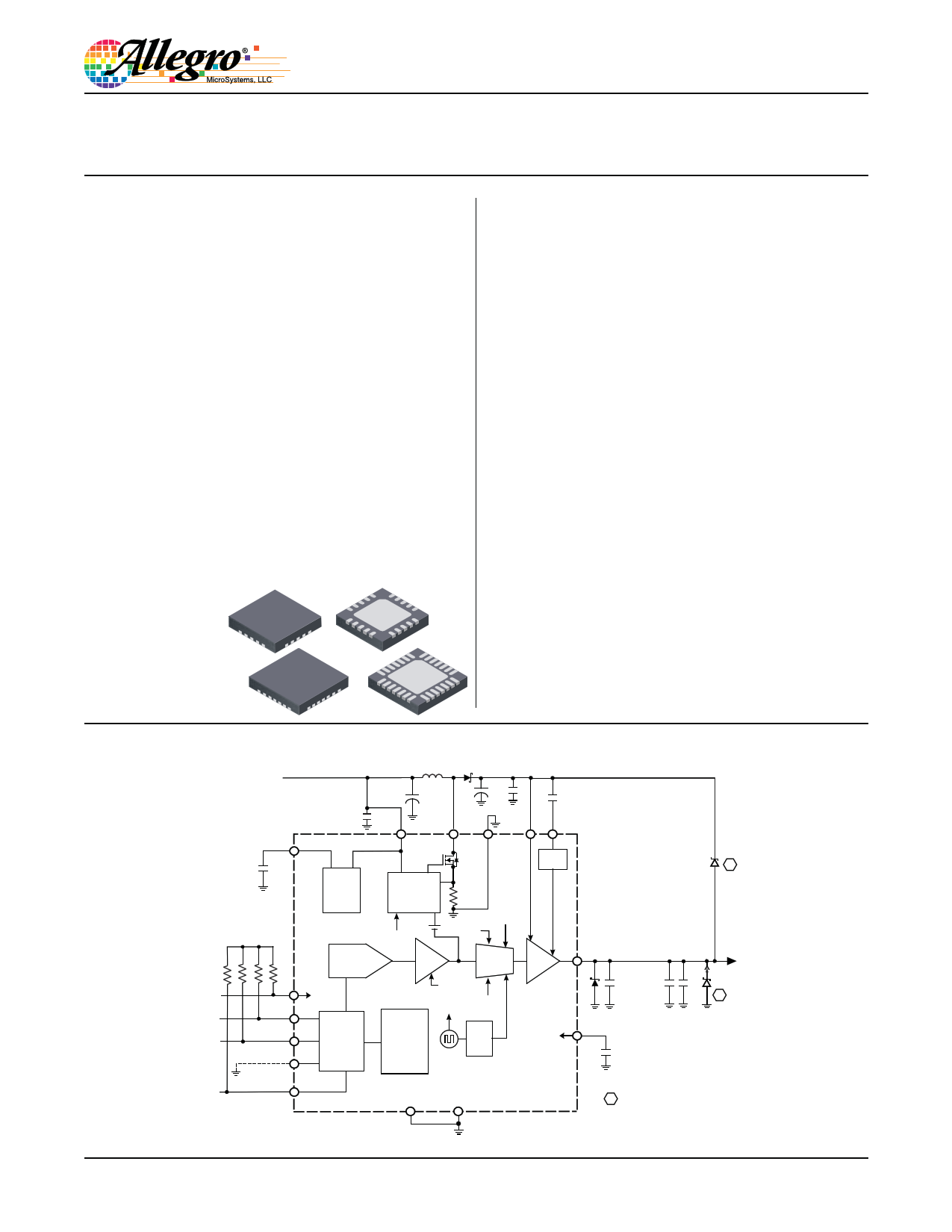
VS
VREG
C3
220 nF
VDD
R1 R2 R3 R4
EXTM
SDA
SCL
ADD
Functional Block Diagram
L1
33 μH
D1
C1
100 nF
C2
100 μF
VIN
C5
100 μF
C6
1 μF
C4
100 nF
LX GNDLX BOOST VCP
Regulator
DAC
I2 C™-
Compatible
Interface
Charge
Pump
D3
A
Boost
Converter
fsw
LNB
Voltage
Control
EXTM
TMode
Wave
Shape
Linear
Stage
TCAP
Fault Monitor
TGate
fsw
OCP
PNG
TSD
VUV
Clock
Divider 22 kHz
Oscillator
LNB
D2
C8
100 nF
C10
220 nF
VOUT
D4
C9
10 nF
A
TCAP
C7
10 nF (or 22 nF)
IRQ
PAD
For recommended external components, refer to table 7
8293-DS, Rev. 4
GND
A D3 and D4 are used for surge protection.
http://www.Datasheet4U.com
1 page 
A8293
Single LNB Supply and Control Voltage Regulator
ELECTRICAL CHARACTERISTICS (continued) at TA = 25°C, VIN = 9 to 16 V, unless noted otherwise1
Characteristics
Symbol
Test Conditions
Min.
Typ. Max.
Tone Duty Cycle
Tone Rise Time
Tone Fall Time
EXTM Logic Input
EXTM Input Leakage
I2C™-Compatible Interface
DCTONE
trTONE
tfTONE
VEXTM(H)
VEXTM(L)
IEXTMLKG
ILOAD = 0 to 450 mA, CLOAD = 750 nF
ILOAD = 0 to 450 mA, CLOAD = 750 nF
ILOAD = 0 to 450 mA, CLOAD = 750 nF
40 50 60
5 10 15
5 10 15
2.0 – –
– – 0.8
–1 – 1
Logic Input (SDA,SCL) Low Level
Logic Input (SDA,SCL) High Level
Logic Input Hysteresis
Logic Input Current
Logic Output Voltage SDA and IRQ
VSCL(L)
VSCL(H)
VI2CIHYS
II2CI
Vt2COut(L)
VI2CI = 0 to 7 V
ILOAD = 3 mA
– – 0.8
2.0 – –
– 150 –
–10 <±1.0 10
– – 0.4
Logic Output Leakage SDA and IRQ
SCL Clock Frequency
Output Fall Time
Bus Free Time Between Stop/Start
Hold Time Start Condition
Setup Time for Start Condition
SCL Low Time
SCL High Time
Data Setup Time
Data Hold Time
Vt2CLKG
fCLK
tfI2COut
tBUF
tHD:STA
tSU:STA
tLOW
tHIGH
tSU:DAT
tHD:DAT
Vt2COut = 0 to 7 V
Vt2COut(H) to Vt2COut(L)
For tHD:DAT(min), the master device must
provide a hold time of at least 300 ns for the
SDA signal in order to bridge the undefined
region of the SCL signal falling edge
–
–
–
1.3
0.6
0.6
1.3
0.6
100
0
– 10
– 400
– 250
––
––
––
––
––
––
– 900
Setup Time for Stop Condition
I2C™ Address Setting
tSU:STO
0.6 – –
ADD Voltage for Address 0001,000
Address1
0 – 0.7
ADD Voltage for Address 0001,001
Address2
1.3 – 1.7
ADD Voltage for Address 0001,010
Address3
2.3 – 2.7
ADD Voltage for Address 0001,011
Address4
3.3 – 5.0
1Operation at 16 V may be limited by power loss in the linear regulator.
2Guaranteed by worst case process simulations and system characterization. Not production tested.
3LNB output ripple and noise are dependent on component selection and PCB layout. Refer to the Application Schematic and PCB layout
recommendations. Not production tested.
4Current from the LNB output may be limited by the choice of Boost components.
Units
%
μs
μs
V
V
μA
V
V
mV
μA
V
μA
kHz
ns
μs
μs
μs
μs
μs
ns
ns
μs
V
V
V
V
I2C™ Interface Timing Diagram
tSU:STA tHD:STA t
SU:DAT t
HD:DAT t
tSU:STO
BUF
SDA
SCL
tLOW
tHIGH
Allegro MicroSystems, LLC
115 Northeast Cutoff
Worcester, Massachusetts 01615-0036 U.S.A.
1.508.853.5000; www.allegromicro.com
5
5 Page 
A8293
Single LNB Supply and Control Voltage Regulator
Table 2. Control Register Address (I1, I0) = 10
Bit Name
Function
0 TMODE
0: External Tone
1: Internal Tone
1 TGATE
0: Tone Gated Off
1: Tone Gated On
2-
Not Used (0 recommended)
3-
Not Used
4-
Not Used
5-
Not Used
6 I0
Address Bit: 0
7 I1
Address Bit: 1
Bit 0 TMODE Tone Mode. Selects between the use of an external 22 kHz logic signal or the use of
the internal 22 kHz oscillator to control the tone generation on the LNB output. A 0
selects the external tone and a 1 selects the internal tone. See the Tone Generation
section for more information
Bit 1 TGATE Tone Gate. Allows either the internal or external 22 kHz tone signals to be gated,
unless the EXTM is selected for gating. When set to 0, the selected tone (via
TMODE) is off. When set to 1, the selected tone is on. See Tone Generation Section
for more information.
Bit 2 –
Not Used.
Bit 3 –
Not Used.
Bit 4 –
Not Used.
Bit 5 –
Not Used.
Bit 6 I0
Address.
Bit 7 I1
Address.
Allegro MicroSystems, LLC
115 Northeast Cutoff
Worcester, Massachusetts 01615-0036 U.S.A.
1.508.853.5000; www.allegromicro.com
11
11 Page | ||
| Páginas | Total 19 Páginas | |
| PDF Descargar | [ Datasheet A8293.PDF ] | |
Hoja de datos destacado
| Número de pieza | Descripción | Fabricantes |
| A8290 | Single LNB Supply and Control Voltage Regulator | Allegro MicroSystems |
| A8290 | LED DRIVER | AiT Semiconductor |
| A8291 | Single LNB Supply and Control Voltage Regulator | Allegro MicroSystems |
| A8292 | Dual LNB Supply and Control Voltage Regulator | Allegro MicroSystems |
| Número de pieza | Descripción | Fabricantes |
| SLA6805M | High Voltage 3 phase Motor Driver IC. |
Sanken |
| SDC1742 | 12- and 14-Bit Hybrid Synchro / Resolver-to-Digital Converters. |
Analog Devices |
|
DataSheet.es es una pagina web que funciona como un repositorio de manuales o hoja de datos de muchos de los productos más populares, |
| DataSheet.es | 2020 | Privacy Policy | Contacto | Buscar |