|
|
|
PDF BD3538F Data sheet ( Hoja de datos )
| Número de pieza | BD3538F | |
| Descripción | Termination Regulators | |
| Fabricantes | ROHM Semiconductor | |
| Logotipo | ||
Hay una vista previa y un enlace de descarga de BD3538F (archivo pdf) en la parte inferior de esta página. Total 20 Páginas | ||
|
No Preview Available !
Datasheet
Termination Regulators for DDR-SDRAMs
BD3538F BD3538HFN
General Description
BD3538F/HFN is a termination regulator that complies
with JEDEC requirements for DDR-SDRAM. This
linear power supply uses a built-in N-channel MOSFET
and high-speed OP-AMPS specially designed to
provide excellent transient response. It has a
sink/source current capability of up to 1A and has a
power supply bias requirements of 3.3V to 5.0V for
driving the N-channel MOSFET. By employing an
independent reference voltage input (VDDQ) and a
feedback pin (VTTS), this termination regulator
provides excellent output voltage accuracy and load
regulation as required by JEDEC standards.
Additionally, BD3538 has a reference power supply
output (VREF) for DDR-SDRAM or a memory
controller. Unlike the VTT output that goes to “Hi-Z”
state, the VREF output is kept unchanged when EN
input is changed to “Low”, making this IC suitable for
DDR-SDRAM under “Self Refresh” state.
Features
Incorporates a push-pull power supply for
termination (VTT)
Incorporates a reference voltage circuit (VREF)
Incorporates an enabler
Incorporates an undervoltage lockout (UVLO)
Incorporates a thermal shutdown protector (TSD)
Compatible with Dual Channel (DDR-II)
Key Specifications
Termination Input Voltage Range:
1.0V to 5.5V
VCC Input Voltage Range:
2.7V to 5.5V
VDDQ Reference Voltage Range: 1.0V to 2.75V
Output Voltage:
1/2 x VVDDQ V(Typ)
Output Current:
1.0A (Max)
High side FET O-Resistance:
0.4Ω(Typ)
Low side FET ON-Resistance:
0.4Ω(Typ)
Standby Current:
0.5mA (Typ)
Operating Temperature Range: -40°C to +105°C
Packages
W(Typ) x D(Typ) x H(Max)
SOP8
5.00mm x 6.20mm x 1.71mm
Applications
Power supply for DDR I / II - SDRAM
HSON8
2.90mm x 3.00mm x 0.60mm
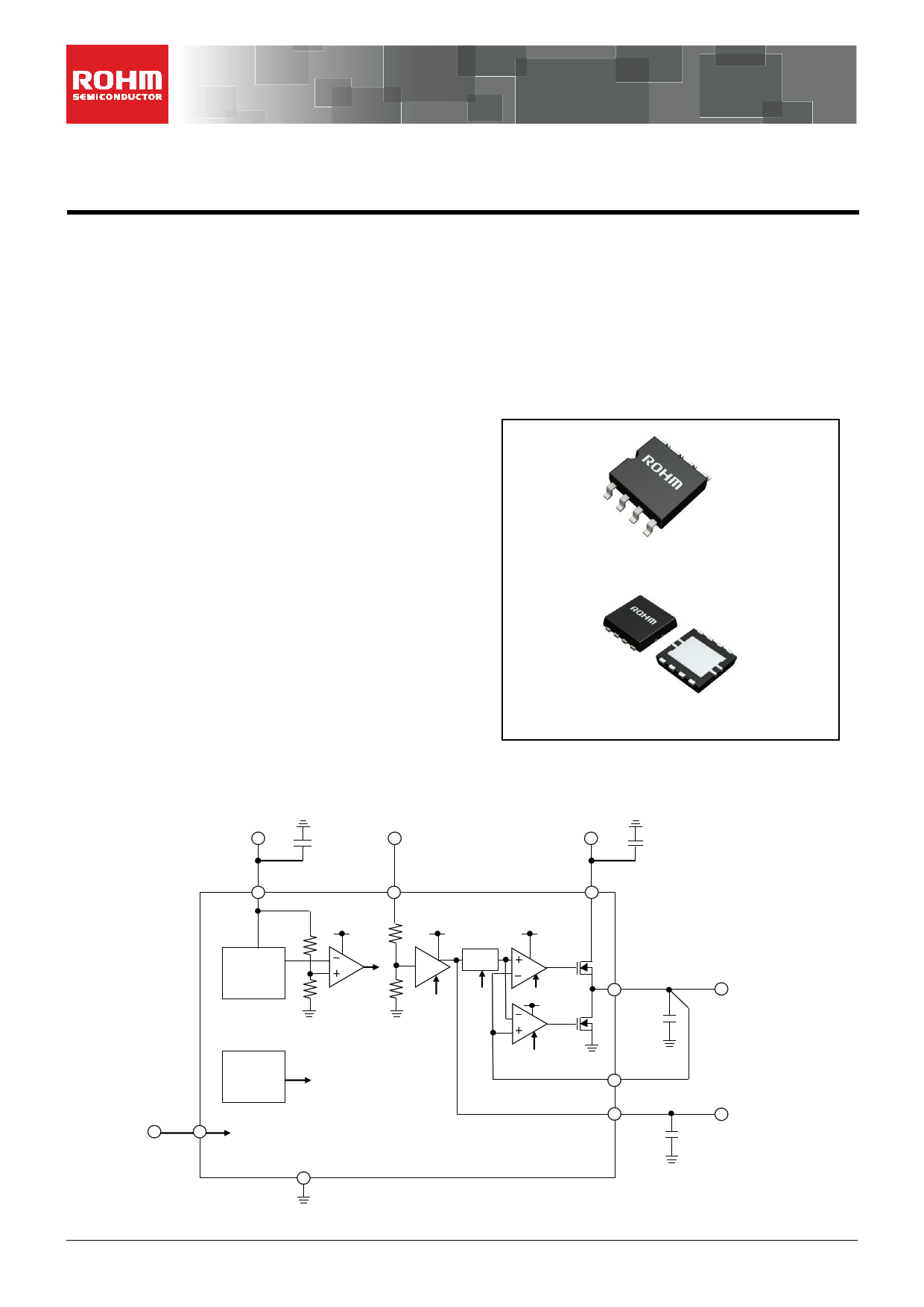
Typical Application Circuit, Block Diagram
VCC
VDDQ
VTT_IN
VCC
6
VCC
VDDQ
5
VCC
VCC
VTT_IN
7
Reference
Block
Thermal TSD
Protection
Enable
EN
2
EN
UVLO
SOFT
UVLO
TSD
EN
UVLO
TSD
VCC EN
UVLO
TSD
EN
UVLO
VTT
8
3
VTTS
4
VREF
VTT
½x
VDDQ
1
GND
○Product structure:Silicon monolithic integrated circuit
.www.rohm.com
© 2015 ROHM Co., Ltd. All rights reserved.
TSZ22111・14・001
○This product has no designed protection against radioactive rays
1/16
TSZ02201-0J2J0A900980-1-2
02.Nov.2015 Rev.001
1 page 
BD3538F BD3538HFN
Typical Waveforms
VVTT(20mV/Div)
IVTT(1A/Div)
10µsec/Div
Figure 1. DDR1
(-1A → +1A)
VVTT(20mV/Div)
IVTT(1A/Div)
10µsec/Div
Figure 3. DDR2
(-1A → +1A)
VVTT(20mV/Div)
IVTT(1A/Div)
10µsec/Div
Figure 2. DDR1
(+1A → -1A)
VVTT(20mV/Div)
IVTT(1A/Div)
10µsec/Div
Figure 4. DDR2
(+1A → -1A)
www.rohm.com
© 2015 ROHM Co., Ltd. All rights reserved.
TSZ22111・15・001
5/16
TSZ02201-0J2J0A900980-1-2
02.Nov.2015 Rev.001
5 Page 
BD3538F BD3538HFN
Operational Notes – continued
12. Regarding the Input Pin of the IC
This monolithic IC contains P+ isolation and P substrate layers between adjacent elements in order to keep them
isolated. P-N junctions are formed at the intersection of the P layers with the N layers of other elements, creating a
parasitic diode or transistor. For example (refer to figure below):
When GND > Pin A and GND > Pin B, the P-N junction operates as a parasitic diode.
When GND > Pin B, the P-N junction operates as a parasitic transistor.
Parasitic diodes inevitably occur in the structure of the IC. The operation of parasitic diodes can result in mutual
interference among circuits, operational faults, or physical damage. Therefore, conditions that cause these diodes to
operate, such as applying a voltage lower than the GND voltage to an input pin (and thus to the P substrate) should
be avoided.
Resistor
Transistor (NPN)
Pin A
Pin A
Pin B
C
B
E
Pin B
P+
NN
Parasitic
Elements
P P+
NN
P Substrate
GND
Parasitic
Elements
N P+
N P N P+ N
P Substrate
Parasitic
GND GND
Elements
Figure 13. Example of monolithic IC structure
B
N Region
close-by
C
E
Parasitic
Elements
GND
13. Thermal Shutdown Circuit(TSD)
This IC has a built-in thermal shutdown circuit that prevents heat damage to the IC. Normal operation should always
be within the IC’s power dissipation rating. If however the rating is exceeded for a continued period, the junction
temperature (Tj) will exceed 175°C which will activate the TSD circuit that will turn OFF all output pins. When the Tj
falls below the TSD threshold, the circuits are automatically restored to normal operation.
Note that the TSD circuit operates in a situation that exceeds the absolute maximum ratings and therefore, under no
circumstances, should the TSD circuit be used in a set design or for any purpose other than protecting the IC from
heat damage.
14. Capacitor Across Output and GND
If a large capacitor is connected between the output pin and ground pin, current from the charged capacitor can flow
into the output pin and may destroy the IC when the VCC or IN pin is shorted to ground or pulled down to 0V. Use a
capacitor smaller than 1000µF between output and ground.
15. Output Capacitor Resistor
Do not fail to connect a output capacitor to VREF output terminal for stabilization of output voltage. The capacitor
connected to VREF output terminal works as a loop gain phase compensator. Insufficient capacitance may cause an
oscillation. It is recommended to use a low temperature coefficient 1-10 µF ceramic capacitor, though it depends on
ambient temperature and load conditions. It is therefore requested to carefully check under the actual temperature
and load conditions to be applied.
16. Output Capacitor
Do not fail to connect a capacitor to VTT output pin for stabilization of output voltage. This output capacitor works as
a loop gain phase compensator and an output voltage variation reducer in the event of sudden change in load.
Insufficient capacitance may cause an oscillation. And if the equivalent series resistance (ESR) of this capacitor is
high, the variation in output voltage increases in the event of sudden change in load. It is recommended to use a 220
µF functional polymer capacitor, though it depends on ambient temperature and load conditions. Using a low ESR
ceramic capacitor may reduce a loop gain phase margin and cause an oscillation, which may be improved by
connecting a resistor in series with the capacitor. It is therefore requested to carefully check under the actual
temperature and load conditions to be applied.
www.rohm.com
© 2015 ROHM Co., Ltd. All rights reserved.
TSZ22111・15・001
11/16
TSZ02201-0J2J0A900980-1-2
02.Nov.2015 Rev.001
11 Page | ||
| Páginas | Total 20 Páginas | |
| PDF Descargar | [ Datasheet BD3538F.PDF ] | |
Hoja de datos destacado
| Número de pieza | Descripción | Fabricantes |
| BD3538F | Termination Regulators | ROHM Semiconductor |
| BD3538FVM | Regulator IC | ROHM Semiconductor |
| BD3538HFN | Termination Regulators | ROHM Semiconductor |
| Número de pieza | Descripción | Fabricantes |
| SLA6805M | High Voltage 3 phase Motor Driver IC. |
Sanken |
| SDC1742 | 12- and 14-Bit Hybrid Synchro / Resolver-to-Digital Converters. |
Analog Devices |
|
DataSheet.es es una pagina web que funciona como un repositorio de manuales o hoja de datos de muchos de los productos más populares, |
| DataSheet.es | 2020 | Privacy Policy | Contacto | Buscar |