|
|
PDF S-1155 Data sheet ( Hoja de datos )
| Número de pieza | S-1155 | |
| Descripción | HIGH RIPPLE-REJECTION LOW DROPOUT HIGH OUTPUT CURRENT CMOS VOLTAGE REGULATOR | |
| Fabricantes | Seiko Instruments | |
| Logotipo |  |
|
Hay una vista previa y un enlace de descarga de S-1155 (archivo pdf) en la parte inferior de esta página. Total 28 Páginas | ||
|
No Preview Available !
Rev.1.1_00
HIGH RIPPLE-REJECTION LOW DROPOUT HIGH OUTPUT CURRENT
CMOS VOLTAGE REGULATOR
S-1155 Series
www.datasheet4u.com
The S-1155 Series, developed based on CMOS technology, is a positive
voltage regulator with a super low dropout voltage, high output voltage
accuracy, and low current consumption.
The S-1155 Series provides the very small dropout voltage and the large
output current due to the built-in transistor with low on-resistance. The
overcurrent protector prevents the load current from exceeding the
capacitance of output transistor. The thermal shutdown circuit prevents
damage caused by heat, the rush current control circuit limits the
excessive rush current during start-up.
The ON/OFF circuit ensures longer battery life. Various capacitors, also
small ceramic capacitors, can be used for this IC more than for the
conventional regulator ICs which have CMOS technology.
The small package SOT-89-5 enables high-density mounting.
Features
• Output voltage :
• Low equivalent series resistance capacitor :
• Input voltage :
• High-accuracy output voltage :
• Low dropout voltage :
• Low current consumption :
• Output current :
• High ripple rejection :
• Built-in overcurrent protection circuit :
• Built-in thermal shutdown circuit :
• Built-in rush current control circuit :
• Built-in power on/off circuit :
• Small package :
• Lead-free product
1.0 to 5.0 V, selectable in 0.05 V step.
Ceramic capacitor of 4.7 µF or more can be used as the
I/O capacitor.
1.5 to 5.5 V
±1.0% (1.0 to 1.45 V output product : ±15 mV)
70 mV typ. (3.0 V output product, at IOUT = 200 mA)
During operation : 70 µA typ., 90 µA max. (3.0 V output
product)
During shutdown : 0.1 µA typ., 1.0 µA max.
500 mA (3.0 V output product, at VIN ≥ VOUT(S) + 1.0 V)*1
70 dB typ. (at 1.0 kHz, VOUT = 1.0 V)
limits overcurrent of output transistor
prevents damage caused by heat
limits excessive rush current during start-up
Longer battery life
SOT-89-5
*1. Attention should be paid to the power dissipation of the package when the output current is large.
Applications
• Power supply for battery-powered devices
• Power supply for TV, notebook PCs and home electric appliances
• Constant-voltage power supply for portable equipment
Packages
Package Name
SOT-89-5
Package
UP005-A
Drawing Code
Tape
UP005-A
Reel
UP005-A
Seiko Instruments Inc.
1
1 page 
Rev.1.1_00
HIGH RIPPLE-REJECTION LOW DROPOUT HIGH OUTPUT CURRENT CMOS VOLTAGE REGULATOR
S-1155 Series
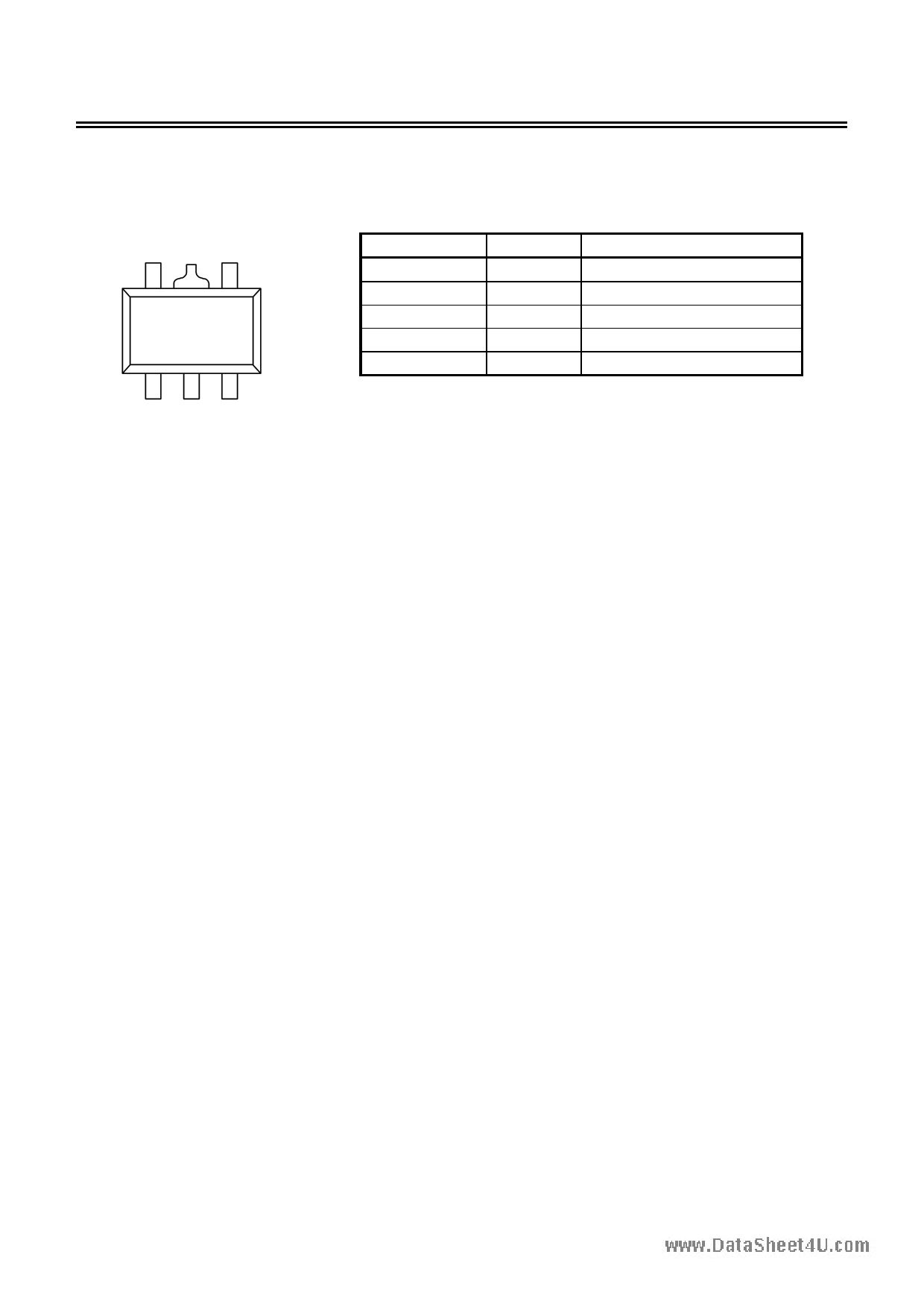
Pin Configuration
SOT-89-5
www.datasheet4u.comTop view
54
12 3
Figure 2
Table 2
Pin No.
Symbol
Description
1 ON/OFF Shutdown pin
2
VSS
GND pin
3
NC*1
No connection
4 VIN Input voltage pin
5
VOUT
Output voltage pin
*1. The NC pin is electrically open.
The NC pin can be connected to VIN or VSS.
Seiko Instruments Inc.
5
5 Page 
Rev.1.1_00
HIGH RIPPLE-REJECTION LOW DROPOUT HIGH OUTPUT CURRENT CMOS VOLTAGE REGULATOR
S-1155 Series
Explanation of Terms
1. Low dropout voltage regulator
www.datasheeTth4uis.cIoCm’s voltage regulator has the low dropout voltage due to its built-in transistor with low on-resistance.
2. Output voltage (VOUT)
The accuracy of the output voltage is ensured at ±1.0% or ±15 mV*2 under the specified conditions of fixed input
voltage*1, fixed output current, and fixed temperature.
*1. Differs depending on the product.
*2. When VOUT < 1.5 V : ±15 mV, When 1.5 V ≤ VOUT : ±1.0%
Caution
If the above conditions change, the output voltage value may vary and exceed the accuracy
range of the output voltage. See “ Electrical Characteristics” and “ Characteristics (Typical
Data)” for details.
3. Line regulation ∆VOUT1
∆VIN • VOUT
Indicates the dependency of the output voltage against the input voltage. That is, the value shows how much the
output voltage changes due to a change in the input voltage after fixing output current constant.
4. Load regulation (∆VOUT2)
Indicates the dependency of the output voltage against the output current. That is, the value shows how much the
output voltage changes due to a change in the output current after fixing output current constant.
5. Dropout voltage (Vdrop)
Indicates the difference between the output voltage and the input voltage VIN1, which is the input voltage (VIN) when;
decreasing input voltage VIN gradually until the output voltage has dropped to the value of 98% of output voltage
VOUT3, which is at VIN = VOUT(S) + 1.0 V or 5.5 V.
Vdrop = VIN1 − (VOUT3 × 0.98)
Seiko Instruments Inc.
11
11 Page | ||
| Páginas | Total 28 Páginas | |
| PDF Descargar | [ Datasheet S-1155.PDF ] | |
Hoja de datos destacado
| Número de pieza | Descripción | Fabricantes |
| S-1155 | HIGH RIPPLE-REJECTION LOW DROPOUT HIGH OUTPUT CURRENT CMOS VOLTAGE REGULATOR | Seiko Instruments |
| Número de pieza | Descripción | Fabricantes |
| SLA6805M | High Voltage 3 phase Motor Driver IC. |
Sanken |
| SDC1742 | 12- and 14-Bit Hybrid Synchro / Resolver-to-Digital Converters. |
Analog Devices |
|
DataSheet.es es una pagina web que funciona como un repositorio de manuales o hoja de datos de muchos de los productos más populares, |
| DataSheet.es | 2020 | Privacy Policy | Contacto | Buscar |
