|
|
PDF ME1117-2.5 Data sheet ( Hoja de datos )
| Número de pieza | ME1117-2.5 | |
| Descripción | 1A Low Dropout Voltage Regulator | |
| Fabricantes | Matsuki | |
| Logotipo |  |
|
Hay una vista previa y un enlace de descarga de ME1117-2.5 (archivo pdf) en la parte inferior de esta página. Total 9 Páginas | ||
|
No Preview Available !
1A Low Dropout Voltage Regulator
GENERAL DESCRIPTION
The ME1117 series of adjustable and fixed voltage regulators are designed to
provide 1A output current and to operate down to 1A input-to-output
differential.
The dropout voltage of the device is guaranteed maximum 1.3V at maximum
output current, decreasing at lower load currents.
On-Chip trimming adjusts the reference voltage to 1%. Current limit is also
trimmed, minimizing the stress under overload conditions on both the
regulator and power source circuitry.
The ME1117 device are pin compatible with other three-triminal SCSI
regulators and are offered in the low profile surface mount SOT-223 package
and in the TO-252(DPAK) and TO-263 plastic package.
TYPICAL APPLICATION
ME1117(Pb-Free)
FEATURES
1. 1.8V, 2.5V, 3.3V, 5.0V, and Adjustable Output
2. Output Current of 1A
3. Operates Down to 1V Dropout
4. Line Regulation : 0.2% Max
5. Output Voltage Tolerance:2% max
6. SOT-223, TO-252 and TO-263 package available.
APPLICATIONS
1. High Efficiency linear Regulators.
2. Post Regulators for Switching Supplies
3. 5V to 3.3V Linear Regulator.
4. Battery Chargers
5. Active SCSI Terminators
6. Power Management for Laptop
7. Battery Powerec Instrumentation
Absolute Maximum Ratings (TA=25℃ Unless Otherwise Noted)
Parameter
Power Dissipation
Input Voltage
Operating Junction Temperature
Storage Temperature
Soldering information Lead Temperature(10 sec)
SOT-223
Thermal Resistance
TO-252
TO-263
Thermal Resistance
SOT-223
TO-252
Symbol
Pd
Vin
θJA
θJC
Limit
Internally
15
-40 to 125
-65 to150
4
90
80
15 to 20
10 to 15
Unit
W
V
℃
℃
Sec
℃/W
℃/W
℃/W
℃/W
℃/W
NOV,2008-Ver2.4
01
1 page 
1A Low Dropout Voltage Regulator
ME1117(Pb-free)
APPLICATION HINTS
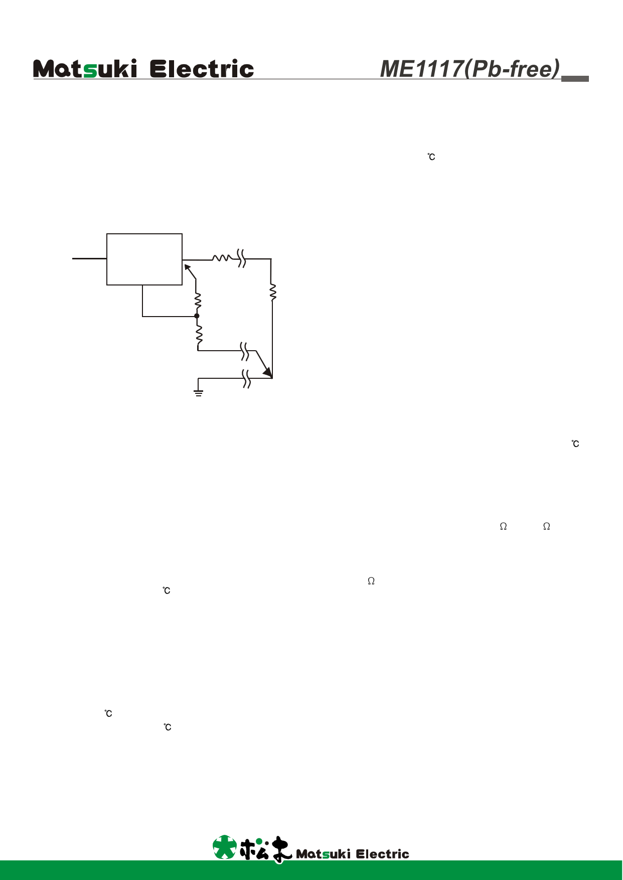
Connected as shown, Rp is not multiplied by the divider ratio
Rp
PARASITIC
ME1117
LINE RESISTANCE
VIN IN OUT
ADJ
R1*
RL
R2*
*CONNECT R1 TO CASE
CONNECT R2 TO CASE
Figure3. Connections for Best Load Regulation
In the case of fixed voltage devices the top of R1 is
connected Kelvin internally, and the ground pin can be
used for negative side sensing.
Thermal Considerations
The ME1117 series have internal power and thermal
limiting circuitry designed to protect the device under
overload conditions. However maximum junction
temperature ratings of 125 should not be exceeded
under continuous normal load conditions.
Careful consideration must be given to all sources of
thermal resistance from junction to ambient. For the
surface mount package SOT-223 additional heat
sources mounted near the device must be considered.
The heat dissipation capability of the PC board and its
copper traces is used as a heat sink for the device. The
thermal resistance from the junction to the tab for the
ME1117 is 15 /W. Thermal resistance from tab to
ambient can be as low as 30 /W.
The total thermal resistance from junction to ambient
can be as low as 45 /W. This requires a reasonable
sized PC board with at least on layer of copper to
spread the heat across the board and couple it into the
surrounding air.Experiments have shown that the heat
spreading copper layer does not need to be electrically
connected to the tab of the device. The PC material can
be very effective at transmitting heat between the pad
area, attached to the pad of the device, and a ground
plane layer either inside or on the opposite side of the
board. Although the actual thermal resistance fo the PC
material is high, the Length/Area ratio of the thermal
resistance between layers is small. For each
application the thermal resistance will be affected by
thermal interactions with other components on the
b o a r d . To d e t e r m i n e t h e a c t u a l v a l u e s o m e
experimentation will be necessary.
The power dissipation of the ME1117 is equal to :
PD=(VIN-VOUT)(IOUT)
Maximum junction temperature will be equal to:
TJ=TA(MAX)+PD(Thermal Resistance(Junction-to-
ambient))
Maximum junction temperature must not exceed 125 .
Ripple Rejection
The ripple rejection values are measured with the
adjustment pin bypassed. The impedance of the adjust
pin capacitor at the ripple frequency should be less
than the value of R1(normally 100 to 200 for a
proper bypassing and ripple rejection approaching the
values shown. The size of the required adjust pin
capacitor is a function of the input ripple frequency. If
R1=100 at 120Hz,the adjust pin capacitor should
be>13uF. At 10kHz only 0.16uF is needed.
The ripple rejection will be a function of output voltage,
in circuits without an adjust pin bypass capacitor. The
output ripple will increase directly as a ratio of the
output voltage to the reference voltage (VOUT/VREF).
05
5 Page | ||
| Páginas | Total 9 Páginas | |
| PDF Descargar | [ Datasheet ME1117-2.5.PDF ] | |
Hoja de datos destacado
| Número de pieza | Descripción | Fabricantes |
| ME1117-2.5 | 1A Low Dropout Voltage Regulator | Matsuki |
| Número de pieza | Descripción | Fabricantes |
| SLA6805M | High Voltage 3 phase Motor Driver IC. |
Sanken |
| SDC1742 | 12- and 14-Bit Hybrid Synchro / Resolver-to-Digital Converters. |
Analog Devices |
|
DataSheet.es es una pagina web que funciona como un repositorio de manuales o hoja de datos de muchos de los productos más populares, |
| DataSheet.es | 2020 | Privacy Policy | Contacto | Buscar |
