|
|
|
PDF MP020-5 Data sheet ( Hoja de datos )
| Número de pieza | MP020-5 | |
| Descripción | Primary-Side Regulator | |
| Fabricantes | MPS | |
| Logotipo | ||
Hay una vista previa y un enlace de descarga de MP020-5 (archivo pdf) en la parte inferior de esta página. Total 20 Páginas | ||
|
No Preview Available !
The Future of Analog IC Technology
DESCRIPTION
The MP020-5 is an offline, primary-side
regulator that provides accurate constant
voltage and constant current regulation without
an opto-coupler or a secondary feedback circuit.
It has an integrated 700V MOSFET.
The MP020-5's variable off-time control allows
a flyback converter to operate in discontinuous
conduction mode. The MP020-5 also features
protection functions such as VCC under-voltage
lockout, over-current protection, over-
temperature protection, open circuit protection
(OCkP) and over-voltage protection. Its internal
high-voltage start-up current source and power-
saving technologies limit the no-load power
consumption to less than 30mW.
The MP020-5's variable-switching-frequency
technology provides natural spectrum shaping
to smooth the EMI signature, making it suitable
for offline, low-power battery chargers and
adapters.
The MP020-5 is available in SOIC8-7A.
Part Num.
MP020-5GS
RON
10Ω
Maximum Output
Power (85-265Vac)
Adapter
Open
Frame
5W 8W
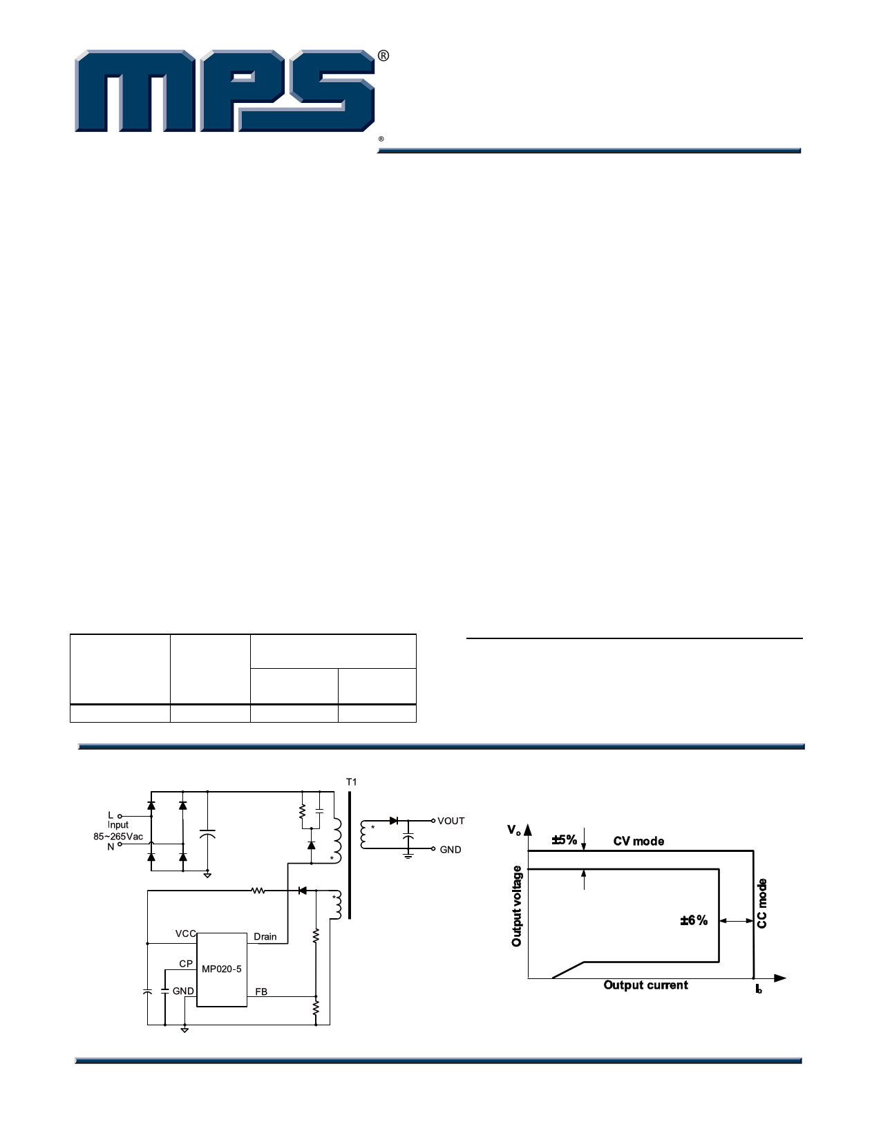
TYPICAL APPLICATION
MP020-5
Offline, Primary-Side Regulator
with CC/CV Control and a 700V FET
FEATURES
• Primary-Side–Control without Opto-Coupler
or Secondary Feedback Circuit
• Precise Constant Current and Constant
Voltage Control (CC/CV)
• Integrated 700V MOSFET with Minimal
External Components
• Variable, Off-Time, Peak-Current Control
• 550µA High-Voltage Current Source
• 30mW No-Load Power Consumption
• Programmable Cable Compensation
• Multiple Protections: OVP, OCP, OCkP,
OTP, and VCC UVLO
• Natural Spectrum Shaping for Improved
EMI Signature
• Low Cost and Simple External circuit
• SOIC8-7A Package
APPLICATIONS
• Cell Phone Chargers
• Adapters for Handheld Electronics
• Stand-By and Auxiliary Power Supplies
• Small Appliances
All MPS parts are lead-free and adhere to the RoHS directive. For MPS green
status, please visit MPS website under Products, Quality Assurance page.
“MPS” and “The Future of Analog IC Technology”, are Registered Trademarks
of Monolithic Power Systems, Inc.
MP020-5 Rev. 1.05
www.MonolithicPower.com
1/23/2014
MPS Proprietary Information. Patent Protected. Unauthorized Photocopy and Duplication Prohibited.
© 2014 MPS. All Rights Reserved.
1
1 page 
MP020-5 – OFFLINE, PRIMARY-SIDE REGULATOR WITH CC/CV CONTROL AND A 700V FET
TYPICAL CHARACTERISTICS (CONTINUED)
OVP Sample Delay vs.
Junction Temperature
On State Resistance vs.
Junction Temperature
5.0 20
4.5
15
4.0
3.5 10
3.0
2.5
2.0
-50 -25 0 25 50 75 100 125
5
0
-50 -25 0 25 50 75 100 125
Current ILimit vs.
Junction Temperature
400
390
380
370
360
350
-50 -25 0 25 50 75 100 125
MP020-5 Rev. 1.05
www.MonolithicPower.com
1/23/2014
MPS Proprietary Information. Patent Protected. Unauthorized Photocopy and Duplication Prohibited.
© 2014 MPS. All Rights Reserved.
5
5 Page 
MP020-5 – OFFLINE, PRIMARY-SIDE REGULATOR WITH CC/CV CONTROL AND A 700V FET
VFB
=
NP _ AU
NS
× (VO
+
VD ) ×
RDOWN
RUP + RDOWN
Where
• VD is the secondary-side-diode forward-drop
voltage,
• Vo is the output voltage,
• NP_AU and NS are the number of auxiliary
winding and secondary side winding turns
(respectively), and
• RUP and RDOWN are the resistor-divider for
sampling.
Figure 5: Auxiliary Voltage Waveform
The output voltage differs from the secondary
voltage due to the current-dependant forward-
diode voltage drop. If the secondary voltage is
always detected at a fixed secondary current,
the difference between the output voltage and
the secondary voltage is a fixed VD. The
MP020-5 samples the auxiliary winding voltage
3.5µs after the primary switch turns off. The CV
loop control function turns the secondary side
diode off to regulate the output voltage.
Constant Current Operation
Figure 6 shows the constant-current operation.
VFB ZCD
Sample
VZCD
IPK Io estimator
VCOMP_I
IO_REF
Figure 6: CC Control Loop
The flyback always works in DCM, and the ZCD
sample block can detect the duty cycle of the
secondary-side diode.
In constant current (CC) operation, the product
of VZCD and Ipk approximately equals IO_REF:
IO _ REF = VZCD × IPK
So, the calculated output current from the IO
estimator block compares with reference value,
IO_REF, and the error signal, VCOMP_I, controls the
turn on signal of the integral MOSFET. So IO is
then.
IO
=
1
2×
NP
NS
× IO _ REF
The MP020-5 maintains IO_REF as 0.152A.
Leading-Edge Blanking
The parasitic capacitances induce a spike on
the sense resistor when the power switch turns
on. The MP020-5 includes a 300ns leading-
edge blanking period to avoid falsely
terminating the switching pulse. During this
blanking period, the current sense comparator
is disabled and the gate driver can not switch
off. Figure 7 shows the leading-edge blanking.
VLimit
tLEB
t
Figure 7: Leading-Edge Blanking
DCM Detection
The MP020-5 operates in discontinuous
conduction mode (DCM) in both CV and CC
modes. To avoid operating in continuous
conduction mode (CCM), the MP020-5 detects
the falling edge of the FB input voltage with
each cycle. If the chip does not detect a 120mV
falling edge, it will stop switching.
MP020-5 Rev. 1.05
www.MonolithicPower.com
1/23/2014
MPS Proprietary Information. Patent Protected. Unauthorized Photocopy and Duplication Prohibited.
© 2014 MPS. All Rights Reserved.
11
11 Page | ||
| Páginas | Total 20 Páginas | |
| PDF Descargar | [ Datasheet MP020-5.PDF ] | |
Hoja de datos destacado
| Número de pieza | Descripción | Fabricantes |
| MP020-5 | Primary-Side Regulator | MPS |
| Número de pieza | Descripción | Fabricantes |
| SLA6805M | High Voltage 3 phase Motor Driver IC. |
Sanken |
| SDC1742 | 12- and 14-Bit Hybrid Synchro / Resolver-to-Digital Converters. |
Analog Devices |
|
DataSheet.es es una pagina web que funciona como un repositorio de manuales o hoja de datos de muchos de los productos más populares, |
| DataSheet.es | 2020 | Privacy Policy | Contacto | Buscar |