|
|
|
PDF CY14B104M Data sheet ( Hoja de datos )
| Número de pieza | CY14B104M | |
| Descripción | 4-Mbit (512 K X 8/256 K X 16) nvSRAM | |
| Fabricantes | Cypress Semiconductor | |
| Logotipo | ||
Hay una vista previa y un enlace de descarga de CY14B104M (archivo pdf) en la parte inferior de esta página. Total 30 Páginas | ||
|
No Preview Available !
CY14B104K, CY14B104M
4-Mbit (512 K × 8/256 K × 16) nvSRAM
with Real Time Clock
Features
■ 25 ns and 45 ns access times
■ Internally organized as 512 K × 8 (CY14B104K) or 256 K × 16
(CY14B104M)
■ Hands off automatic STORE on power-down with only a small
capacitor
■ STORE to QuantumTrap nonvolatile elements is initiated by
software, device pin, or AutoStore on power-down
■ RECALL to SRAM is initiated by software or power-up
■ High reliability
■ Infinite read, write, and RECALL cycles
■ 1 million STORE cycles to QuantumTrap
■ 20 year data retention
■ Single 3-V +20%, –10% operation
■ Data integrity of Cypress nvSRAM combined with full-featured
real time clock (RTC)
■ Watchdog timer
■ Clock alarm with programmable interrupts
■ Capacitor or battery backup for RTC
■ Industrial temperature
■ 44-pin and 54-pin thin small outline package (TSOP II)
■ Pb-free and restriction of hazardous substances (RoHS)
compliant
Functional Description
The Cypress CY14B104K and CY14B104M combines a 4-Mbit
nonvolatile static RAM (nvSRAM) with a full-featured RTC in a
monolithic integrated circuit. The embedded nonvolatile
elements incorporate QuantumTrap technology producing the
world’s most reliable nonvolatile memory. The SRAM is read and
written infinite number of times, while independent nonvolatile
data resides in the nonvolatile elements.
The RTC function provides an accurate clock with leap year
tracking and a programmable, high accuracy oscillator. The
alarm function is programmable for periodic minutes, hours,
days, or months alarms. There is also a programmable watchdog
timer for process control.
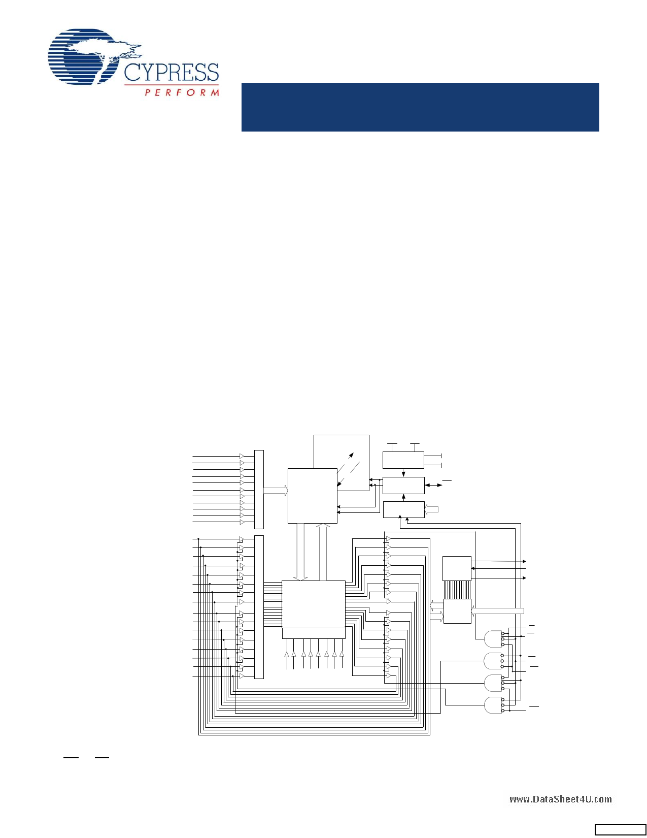
Logic Block Diagram[1, 2, 3]
www.DataSheet4U.com
A0
A1
A2
A3
A4
A5
A6
A7
A8
A17
A18
DQ0
DQ1
DQ2
DQ3
DQ4
DQ5
DQ6
DQ7
DQ8
DQ9
DQ10
DQ11
DQ12
DQ13
DQ14
DQ15
Quatrum
Trap
VCC
VCA
P
2048 X 2048
R
O
STORE
POWER
CONTROL
VRTCbat
VRTCcap
W RECALL
D
E STATIC RAM
C ARRAY
O 2048 X 2048
D
E
R
STORE/RECALL
CONTROL
SOFTWARE
DETECT
HSB
A14 - A2
I
N
P
U
T
B COLUMN I/O
U
F
F
E
R COLUMN DEC
S
A9 A10 A11 A12 A13 A14 A15 A16
RTC
MUX
Xout
Xin
INT
A18- A0
OE
WE
CE
BLE
Notes
1. Address A0 - A18 for ×8 configuration and Address A0 - A17 for ×16 configuration.
2. Data DQ0 - DQ7 for ×8 configuration and Data DQ0 - DQ15 for ×16 configuration.
3. BHE and BLE are applicable for ×16 configuration only.
Cypress Semiconductor Corporation • 198 Champion Court
Document #: 001-07103 Rev. *S
BHE
• San Jose, CA 95134-1709 • 408-943-2600
Revised January 21, 2011
[+] Feedback
1 page 
CY14B104K, CY14B104M
Figure 2 on page 4 shows the proper connection of the storage
capacitor (VCAP) for automatic STORE operation. Refer to DC
Electrical Characteristics on page 16 for the size of the VCAP. The
voltage on the VCAP pin is driven to VCC by a regulator on the
chip. A pull-up should be placed on WE to hold it inactive during
power-up. This pull-up is effective only if the WE signal is tristate
during power-up. Many MPUs tristate their controls on power-up.
This should be verified when using the pull-up. When the
nvSRAM comes out of power-on-RECALL, the MPU must be
active or the WE held inactive until the MPU comes out of reset.
To reduce unnecessary nonvolatile STOREs, AutoStore, and
Hardware STORE operations are ignored unless at least one
write operation has taken place since the most recent STORE or
RECALL cycle. Software initiated STORE cycles are performed
regardless of whether a write operation has taken place. The
HSB signal is monitored by the system to detect if an AutoStore
cycle is in progress.
Hardware STORE (HSB) Operation
The CY14B104K/CY14B104M provides the HSB pin to control
and acknowledge the STORE operations. The HSB pin is used
to request a Hardware STORE cycle. When the HSB pin is driven
LOW, the CY14B104K/CY14B104M conditionally initiates a
STORE operation after tDELAY. An actual STORE cycle begins
only if a write to the SRAM has taken place since the last STORE
or RECALL cycle. The HSB pin also acts as an open drain driver
(internal 100 k weak pull-up resistor) that is internally driven
LOW to indicate a busy condition when the STORE (initiated by
any means) is in progress.
Note After each Hardware and Software STORE operation HSB
is driven HIGH for a short time (tHHHD) with standard output high
current and then remains HIGH by internal 100 k pull-up
resistor.
SRAM write operations that are in progress when HSB is driven
LOW by any means are given time (tDELAY) to complete before
the STORE operation is initiated. However, any SRAM write
cycles requested after HSB goes LOW are inhibited until HSB
returns HIGH. In case the write latch is not set, HSB is not driven
LOW by the CY14B104K/CY14B104M. But any SRAM read and
write cycles are inhibited until HSB is returned HIGH by MPU or
other external source.
During any STORE operation, regardless of how it is initiated,
the CY14B104K/CY14B104M continues to drive the HSB pin
LOW, releasing it only when the STORE is complete. Upon
completion of the STORE operation, the nvSRAM memory
access is inhibited for tLZHSB time after HSB pin returns HIGH.
Leave the HSB unconnected if it is not used.
Hardware RECALL (Power-Up)
During power-up or after any low power condition
www(VVC.DCCCaa<tagVSahSineWeeItTx4CcUHe.)ec,odamsntihneteVrnSaWl IRTCEHCoAnLLporewqeureuspt,
is
a
latched. When
RECALL cycle
is automatically initiated and takes tHRECALL to complete. During
this time, the HSB pin is driven LOW by the HSB driver and all
reads and writes to nvSRAM are inhibited.
Software STORE
Data is transferred from the SRAM to the nonvolatile memory by
a software address sequence. The CY14B104K/CY14B104M
Software STORE cycle is initiated by executing sequential CE or
OE controlled read cycles from six specific address locations in
exact order. During the STORE cycle, an erase of the previous
nonvolatile data is first performed, followed by a program of the
nonvolatile elements. After a STORE cycle is initiate, further
input and output are disabled until the cycle is completed.
Because a sequence of reads from specific addresses is used
for STORE initiation, it is important that no other read or write
accesses intervene in the sequence, or the sequence is aborted
and no STORE or RECALL takes place. To initiate the Software
STORE cycle, the following read sequence must be performed:
1. Read address 0x4E38 Valid READ
2. Read address 0xB1C7 Valid READ
3. Read address 0x83E0 Valid READ
4. Read address 0x7C1F Valid READ
5. Read address 0x703F Valid READ
6. Read address 0x8FC0 Initiate STORE cycle
The software sequence may be clocked with CE controlled reads
or OE controlled reads, with WE kept HIGH for all the six READ
sequences. After the sixth address in the sequence is entered,
the STORE cycle commences and the chip is disabled. HSB is
driven LOW. After the tSTORE cycle time is fulfilled, the SRAM is
activated again for the read and write operation.
Software RECALL
Data is transferred from the nonvolatile memory to the SRAM by
a software address sequence. A software RECALL cycle is
initiated with a sequence of read operations in a manner similar
to the Software STORE initiation. To initiate the RECALL cycle,
perform the following sequence of CE or OE controlled read
operations:
1. Read address 0x4E38 Valid READ
2. Read address 0xB1C7 Valid READ
3. Read address 0x83E0 Valid READ
4. Read address 0x7C1F Valid READ
5. Read address 0x703F Valid READ
6. Read address 0x4C63 Initiate RECALL cycle
Internally, RECALL is a two step procedure. First, the SRAM data
is cleared; then, the nonvolatile information is transferred into the
SRAM cells. After the tRECALL cycle time, the SRAM is again
ready for read and write operations. The RECALL operation
does not alter the data in the nonvolatile elements.
Document #: 001-07103 Rev. *S
Page 5 of 33
[+] Feedback
5 Page 
CY14B104K, CY14B104M
Table 4. RTC Register Map[9]
Register
CY14B104K CY14B104M
0x7FFFF
0x3FFFF
0x7FFFE
0x3FFFE
D7
0
0x7FFFD
0x7FFFC
0x7FFFB
0x7FFFA
0x7FFF9
0x7FFF8
0x3FFFD
0x3FFFC
0x3FFFB
0x3FFFA
0x3FFF9
0x3FFF8
0
0
0
0
0
OSCEN
(0)
0x7FFF7
0x7FFF6
0x3FFF7
0x3FFF6
WDS
(0)
WIE (0)
0x7FFF5
0x3FFF5
M (1)
BCD Format Data[10]
D6 D5 D4 D3 D2 D1 D0
10s years
Years
0 0 10s
months
Months
0 10s day of month
Day of month
00 0 0
Day of week
0 10s hours
Hours
10s minutes
Minutes
10s seconds
Seconds
0 Cal
sign
(0)
Calibration (00000)
WDW (0)
WDT (000000)
AIE (0)
0
PFE 0
(0)
10s alarm date
H/L P/L (0)
(1)
0
Alarm day
0
0x7FFF4
0x7FFF3
0x3FFF4
0x3FFF3
M (1)
M (1)
0 10s alarm hours
10 alarm minutes
Alarm hours
Alarm minutes
0x7FFF2
0x3FFF2
M (1)
10 alarm seconds
Alarm, seconds
0x7FFF1
0x7FFF0
0x3FFF1
0x3FFF0
WDF
10s Centuries
Centuries
AF PF OSCF[12] 0 CAL (0) W (0) R (0)
Function/Range
Years: 00–99
Months: 01–12
Day of month: 01–31
Day of week: 01–07
Hours: 00–23
Minutes: 00–59
Seconds: 00–59
Calibration values [11]
Watchdog [11]
Interrupts [11]
Alarm, day of month:
01–31
Alarm, hours: 00–23
Alarm, minutes:
00–59
Alarm, seconds:
00–59
Centuries: 00–99
Flags[11]
www.DataSheet4U.com
Notes
9. Upper byte D15-D8 (CY14B104M) of RTC registers are reserved for future use.
10. ( ) designates values shipped from the factory.
11. This is a binary value, not a BCD value.
12. When user resets OSCF flag bit, the flags register will be updated after tRTCp time.
Document #: 001-07103 Rev. *S
Page 11 of 33
[+] Feedback
11 Page | ||
| Páginas | Total 30 Páginas | |
| PDF Descargar | [ Datasheet CY14B104M.PDF ] | |
Hoja de datos destacado
| Número de pieza | Descripción | Fabricantes |
| CY14B104K | 4-Mbit (512 K X 8/256 K X 16) nvSRAM | Cypress Semiconductor |
| CY14B104L | 4-Mbit (512K x 8/256K x 16) nvSRAM | Cypress Semiconductor |
| CY14B104LA | 4-Mbit (512 K X 8/256 K X 16) nvSRAM | Cypress Semiconductor |
| CY14B104M | 4-Mbit (512 K X 8/256 K X 16) nvSRAM | Cypress Semiconductor |
| Número de pieza | Descripción | Fabricantes |
| SLA6805M | High Voltage 3 phase Motor Driver IC. |
Sanken |
| SDC1742 | 12- and 14-Bit Hybrid Synchro / Resolver-to-Digital Converters. |
Analog Devices |
|
DataSheet.es es una pagina web que funciona como un repositorio de manuales o hoja de datos de muchos de los productos más populares, |
| DataSheet.es | 2020 | Privacy Policy | Contacto | Buscar |