|
|
|
PDF BH616UV1611 Data sheet ( Hoja de datos )
| Número de pieza | BH616UV1611 | |
| Descripción | Ultra Low Power/High Speed CMOS SRAM | |
| Fabricantes | Brilliance Semiconductor | |
| Logotipo | ||
Hay una vista previa y un enlace de descarga de BH616UV1611 (archivo pdf) en la parte inferior de esta página. Total 12 Páginas | ||
|
No Preview Available !
Ultra Low Power/High Speed CMOS SRAM
1M X 16 bit / 2M x 8-bit
Pb-Free and Green package materials are compliant to RoHS
BH616UV1611www.DataSheet4U.com
n FEATURES
Ÿ Wide VCC low operation voltage : 1.65V ~ 3.6V
Ÿ Ultra low power consumption :
VCC = 3.6V Operation current : 10mA (Max.) at 55ns
2mA (Max.) at 1MHz
Standby current : 5.0uA (Typ.) at 3.0V/25OC
VCC = 1.2V Data retention current : 1.5uA(Typ.) at 25OC
Ÿ High speed access time :
-55 55ns (Max.) at VCC=1.65~3.6V
-70 70ns (Max.) at VCC=1.65~3.6V
Ÿ Automatic power down when chip is deselected
Ÿ Easy expansion with CE1, CE2 and OE options
Ÿ I/O Configuration x8/x16 selectable by LB and UB pin.
Ÿ Three state outputs and TTL compatible
Ÿ Fully static operation, no clock, no refresh
Ÿ Data retention supply voltage as low as 1.0V
n DESCRIPTION
The BH616UV1611 is a high performance, ultra low power CMOS
Static Random Access Memory organized as 1,048,576 by 16 bits
and operates in a wide range of 1.65V to 3.6V supply voltage.
Advanced CMOS technology and circuit techniques provide both
high speed and low power features with typical operating current of
1.5mA at 1MHz at 3.0V/25OC and maximum access time of 55ns at
1.65V/85OC.
Easy memory expansion is provided by an active LOW chip enable
(CE1), an active HIGH chip enable (CE2) and active LOW output
enable (OE) and three-state output drivers.
The BH616UV1611 has an automatic power down feature, reducing
the power consumption significantly when chip is deselected.
The BH616UV1611 is available in DICE form, JEDEC standard
48-pin TSOP-I and 48-ball BGA package.
n POWER CONSUMPTION
PRODUCT
FAMILY
OPERATING
TEMPERATURE
STANDBY
(ICCSB1, Max)
VCC=3.6V VCC=1.8V
BH616UV1611DI
BH616UV1611BI
BH616UV1611TI
Industrial
-40OC to +85OC
30uA
25uA
POWER DISSIPATION
1MHz
VCC=3.6V
10MHz
Operating
(ICC, Max)
fMax.
1MHz
VCC=1.8V
10MHz
2mA 6mA 10mA 1.5mA 5mA
fMax.
8mA
PKG TYPE
DICE
BGA-48-0810
TSOP I-48
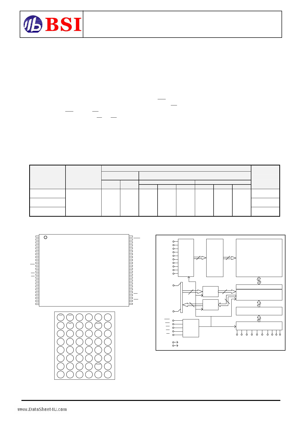
n PIN CONFIGURATIONS
n BLOCK DIAGRAM
A15 1
A14 2
A13 3
A12 4
A11 5
A10 6
A9 7
A8 8
A19 9
NC 10
WE 11
CE2 12
NC 13
UB 14
LB 15
A18 16
A17 17
A7 18
A6 19
A5 20
A4 21
A3 22
A2 23
A1 24
BH616UV1611TI
123456
A LB OE A0 A1 A2 CE2
B DQ8 UB A3 A4 CE1 DQ0
C DQ9 DQ10 A5 A6 DQ1 DQ2
D VSS DQ11 A17 A7 DQ3 VCC
E VCC DQ12 NC A16 DQ4 VSS
F DQ14 DQ13 A14 A15 DQ5 DQ6
G DQ15 A19 A12 A13 WE DQ7
H A18 A8 A9 A10 A11 NC
48 A16
47 BYTE
46 VSS
45 DQ15/A20
44 DQ7
43 DQ14
42 DQ6
41 DQ13
40 DQ5
39 DQ12
38 DQ4
37 VCC
36 DQ11
35 DQ3
34 DQ10
33 DQ2
32 DQ9
31 DQ1
30 DQ8
29 DQ0
28 OE
27 VSS
26 CE1
25 A0
A15
A14
A13
A12
A11
A10
A9
A8
A19
A18
DQ0
.
.
.
.
.
.
DQ15
CE2, CE1
WE
OE
UB
LB
VCC
VSS
Address
Input
Buffer
10
. 16
.
.
. 16
.
.
Control
Row
Decoder
1024
Memory Array
1024 x 16384
Data
Input
Buffer
Data
Output
Buffer
16
16
16384
Column I/O
Write Driver
Sense Amp
1024
Column Decoder
10
Address Input Buffer
A16 A0 A17 A7 A6 A5 A4 A3 A2 A1
48-ball BGA top view
Brilliance Semiconductor, Inc. reserves the right to change products and specifications without notice.
Detailed product characteristic test report is available upon request and being accepted.
R0201-BH616UV1611
1
Revision 1.3
Otc. 2006
1 page 
n DATA RETENTION CHARACTERISTICS (TA = -40OC to +85OC)
BH616UV1611www.DataSheet4U.com
SYMBOL
VDR
ICCDR
tCDR
tR
PARAMETER
TEST CONDITIONS
VCC for Data Retention
Data Retention Current
CE1≧VCC-0.2V or CE2≦0.2V,
VIN≧VCC-0.2V or VIN≦0.2V
CE1≧VCC-0.2V or CE2≦0.2V,
VIN≧VCC-0.2V or VIN≦0.2V
VCC=1.2V
Chip Deselect to Data
Retention Time
See Retention Waveform
Operation Recovery Time
MIN.
1.0
--
0
tRC (2)
TYP. (1)
--
1.5
--
--
MAX.
--
UNITS
V
15 uA
-- ns
-- ns
1. Typical characteristics are at TA=25OC and not 100% tested.
2. tRC = Read Cycle Time.
n LOW VCC DATA RETENTION WAVEFORM (1) (CE1 Controlled)
VCC
CE1
VCC
tCDR
VIH
Data Retention Mode
VDR≧1.0V
CE1≧VCC - 0.2V
VCC
tR
VIH
n LOW VCC DATA RETENTION WAVEFORM (2) (CE2 Controlled)
VCC
VCC
tCDR
Data Retention Mode
VDR≧1.0V
CE2
CE2≦0.2V
VIL
VCC
tR
VIL
n AC TEST CONDITIONS
(Test Load and Input/Output Reference)
Input Pulse Levels
VCC / 0V
Input Rise and Fall Times
1V/ns
Input and Output Timing
Reference Level
Output Load
tCLZ1, tCLZ2, tBE, tOLZ, tCHZ1,
tCHZ2, tBDO, tOHZ, tWHZ, tOW
Others
0.5Vcc
CL = 5pF+1TTL
CL = 30pF+1TTL
Output
1 TTL
CL(1)
VCC
GND
ALL INPUT PULSES
90%
10%
→←
Rise Time:
1V/ns
90%
10%
→←
Fall Time:
1V/ns
1. Including jig and scope capacitance.
n KEY TO SWITCHING WAVEFORMS
WAVEFORM INPUTS
OUTPUTS
MUST BE
STEADY
MAY CHANGE
FROM “H” TO “L”
MAY CHANGE
FROM “L” TO “H”
DON’T CARE
ANY CHANGE
PERMITTED
DOES NOT
APPLY
MUST BE
STEADY
WILL BE CHANGE
FROM “H” TO “L”
WILL BE CHANGE
FROM “L” TO “H”
CHANGE :
STATE UNKNOW
CENTER LINE IS
HIGH INPEDANCE
“OFF” STATE
R0201-BH616UV1611
5
Revision 1.3
Otc. 2006
5 Page 
n PACKAGE DIMENSIONS
BH616UV1611www.DataSheet4U.com
TSOP I-48 Pin (12mm x 20mm)
R0201-BH616UV1611
11
Revision 1.3
Otc. 2006
11 Page | ||
| Páginas | Total 12 Páginas | |
| PDF Descargar | [ Datasheet BH616UV1611.PDF ] | |
Hoja de datos destacado
| Número de pieza | Descripción | Fabricantes |
| BH616UV1610 | Ultra Low Power/High Speed CMOS SRAM | Brilliance Semiconductor |
| BH616UV1611 | Ultra Low Power/High Speed CMOS SRAM | Brilliance Semiconductor |
| Número de pieza | Descripción | Fabricantes |
| SLA6805M | High Voltage 3 phase Motor Driver IC. |
Sanken |
| SDC1742 | 12- and 14-Bit Hybrid Synchro / Resolver-to-Digital Converters. |
Analog Devices |
|
DataSheet.es es una pagina web que funciona como un repositorio de manuales o hoja de datos de muchos de los productos más populares, |
| DataSheet.es | 2020 | Privacy Policy | Contacto | Buscar |