|
|
|
PDF CY14B104N Data sheet ( Hoja de datos )
| Número de pieza | CY14B104N | |
| Descripción | 4-Mbit (512K x 8/256K x 16) nvSRAM | |
| Fabricantes | Cypress Semiconductor | |
| Logotipo | ||
Hay una vista previa y un enlace de descarga de CY14B104N (archivo pdf) en la parte inferior de esta página. Total 22 Páginas | ||
|
No Preview Available !
PRELIMINARY
CY14B104L, CY14B104N
4-Mbit (512K x 8/256K x 16) nvSRAM
Features
■ 15 ns, 25 ns, and 45 ns access times
■ Internally organized as 512K x 8 (CY14B104L) or 256K x 16
(CY14B104N)
■ Hands off automatic STORE on power down with only a small
capacitor
www.DataSheet4U.com
■ STORE to
QuantumTrap®
nonvolatile
elements
initiated
by
software, device pin or AutoStore® on power down
■ RECALL to SRAM initiated by software or power up
■ Infinite read, write, and recall cycles
■ 8 mA typical ICC at 200 ns cycle time
■ 200,000 STORE cycles to QuantumTrap
■ 20 year data retention
■ Single 3V +20%, –10% operation
■ Commercial and industrial temperatures
■ FBGA and TSOP - II packages
■ RoHS compliance
Functional Description
The Cypress CY14B104L/CY14B104N is a fast static RAM, with
a nonvolatile element in each memory cell. The memory is
organized as 512K words of 8 bits each or 256K words of 16 bits
each. The embedded nonvolatile elements incorporate
QuantumTrap technology, producing the world’s most reliable
nonvolatile memory. The SRAM provides infinite read and write
cycles, while independent nonvolatile data resides in the highly
reliable QuantumTrap cell. Data transfers from the SRAM to the
nonvolatile elements (the STORE operation) takes place
automatically at power down. On power up, data is restored to
the SRAM (the RECALL operation) from the nonvolatile memory.
Both the STORE and RECALL operations are also available
under software control.
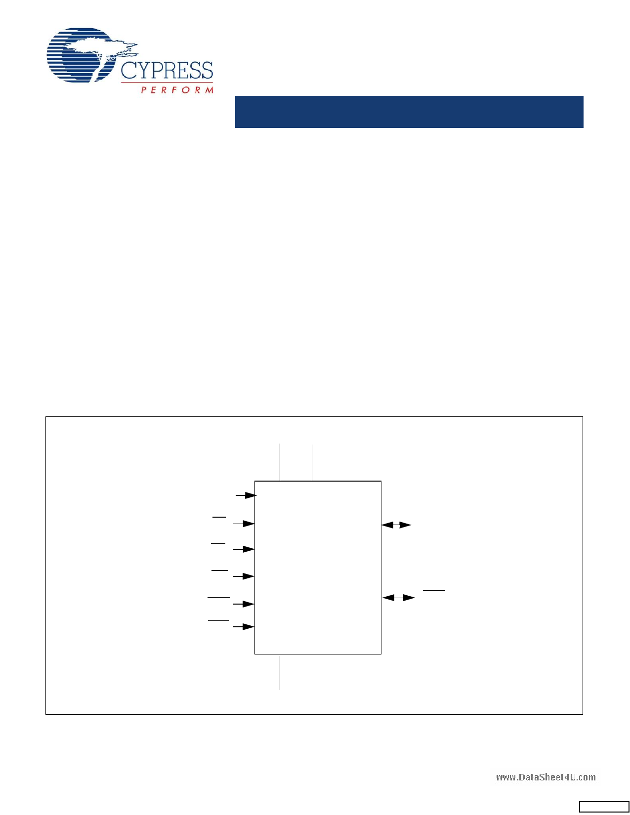
Logic Block Diagram
VCC VCAP
[1]
Address A0 - A18
CE
OE
WE
BHE
BLE
CY14B104L
CY14B104N
[1]
DQ0 - DQ7
HSB
VSS
Note
1. Address A0 - A18 and Data DQ0 - DQ7 for x8 configuration, Address A0 - A17 and Data DQ0 - DQ15 for x16 configuration.
Cypress Semiconductor Corporation • 198 Champion Court
Document #: 001-07102 Rev. *F
• San Jose, CA 95134-1709 • 408-943-2600
Revised January 02, 2008
[+] Feedback
1 page 
PRELIMINARY
CY14B104L, CY14B104N
Hardware RECALL (Power Up)
During power up or after any low power condition
(VCC< VSWITCH), an internal RECALL request is latched. When
VCC again exceeds the sense voltage of VSWITCH, a RECALL
cycle is automatically initiated and takes tHRECALL to complete.
Software STORE
Transfer data from the SRAM to the nonvolatile memory with a
software address sequence. The CY14B104L/CY14B104N
software STORE cycle is initiated by executing sequential
CE-controlled READ cycles from six specific address locations
www.DataShieneet4xUa.cctoomrder. During the STORE cycle an erase of the previous
nonvolatile data is first performed, followed by a program of the
nonvolatile elements. After a STORE cycle is initiated, further
input and output are disabled until the cycle is completed.
Because a sequence of READs from specific addresses is used
for STORE initiation, it is important that no other READ or WRITE
accesses intervene in the sequence. If there are intervening
READ or WRITE accesses, the sequence is aborted and no
STORE or RECALL takes place.
To initiate the software STORE cycle, the following READ
sequence must be performed.
1. Read Address 0x4E38 Valid READ
2. Read Address 0xB1C7 Valid READ
3. Read Address 0x83E0 Valid READ
4. Read Address 0x7C1F Valid READ
5. Read Address 0x703F Valid READ
6. Read Address 0x8FC0 Initiate STORE Cycle
The software sequence may be clocked with CE controlled
READs or OE controlled READs. After the sixth address in the
sequence is entered, the STORE cycle commences and the chip
is disabled. It is important to use READ cycles and not WRITE
cycles in the sequence, although it is not necessary that OE be
LOW for a valid sequence. After the tSTORE cycle time is fulfilled,
the SRAM is activated again for the READ and WRITE operation.
Software RECALL
Transfer the data from the nonvolatile memory to the SRAM with
a software address sequence. A software RECALL cycle is
initiated with a sequence of READ operations in a manner similar
to the software STORE initiation. To initiate the RECALL cycle,
the following sequence of CE controlled READ operations must
be performed.
1. Read Address 0x4E38 Valid READ
2. Read Address 0xB1C7 Valid READ
3. Read Address 0x83E0 Valid READ
4. Read Address 0x7C1F Valid READ
5. Read Address 0x703F Valid READ
6. Read Address 0x4C63 Initiate RECALL Cycle
Internally, RECALL is a two step procedure. First, the SRAM data
is cleared and then, the nonvolatile information is transferred into
the SRAM cells. After the tRECALL cycle time, the SRAM is again
ready for READ and WRITE operations. The RECALL operation
does not alter the data in the nonvolatile elements.
Table 1. Mode Selection
CE WE
HX
LH
LL
LH
LH
OE
A15 - A0
Mode
IO
Power
X
X
Not Selected Output High Z
Standby
L
X
Read SRAM
Output Data
Active
X
X
Write SRAM
Input Data
Active
L
0x4E38
Read SRAM
Output Data
Active[4,5,6]
0xB1C7
Read SRAM
Output Data
0x83E0
Read SRAM
Output Data
0x7C1F
Read SRAM
Output Data
0x703F
Read SRAM
Output Data
0x8B45
AutoStore
Output Data
Disable
L
0x4E38
Read SRAM
Output Data
Active[4,5,6]
0xB1C7
Read SRAM
Output Data
0x83E0
Read SRAM
Output Data
0x7C1F
Read SRAM
Output Data
0x703F
Read SRAM
Output Data
0x4B46
AutoStore Enable Output Data
Notes
4. The six consecutive address locations must be in the order listed. WE must be HIGH during all six cycles to enable a nonvolatile cycle.
5. While there are 19 address lines on the CY14B104L/CY14B104N, only the lower 16 lines are used to control software modes.
6. IO state depends on the state of OE. The IO table shown assumes OE LOW.
Document #: 001-07102 Rev. *F
Page 5 of 22
[+] Feedback
5 Page 
PRELIMINARY
CY14B104L, CY14B104N
Switching Waveforms (continued)
Figure 6. SRAM Read Cycle #2: CE and OE Controlled[10, 21, 23]
ADDRESS
CE
www.DataSheet4U.com
OE
BHE , BLE
DQ (DATA OUT)
tRC
tLZCE
tACE
tDOE
tLZOE
tDBE
tLZBE
tPD
tHZCE
t HZOE
tHZCE
tHZBE
DATA VALID
tPU ACTIVE
ICC STANDBY
ADDRESS
CE
WE
BHE , BLE
DATA IN
DATA OUT
Figure 7. SRAM Write Cycle #1: WE Controlled[21, 22, 23]
tWC
tSA
tSCE
tAW
tPWE
tHA
tBW
PREVIOUS DATA
tHZWE
tSD
DATA VALID
HIGH IMPEDANCE
tHD
tLZWE
Notes
22. CE or WE must be >VIH during address transtions.
23. BHE and BLE are applicable for x16 configuration only.
Document #: 001-07102 Rev. *F
Page 11 of 22
[+] Feedback
11 Page | ||
| Páginas | Total 22 Páginas | |
| PDF Descargar | [ Datasheet CY14B104N.PDF ] | |
Hoja de datos destacado
| Número de pieza | Descripción | Fabricantes |
| CY14B104K | 4-Mbit (512 K X 8/256 K X 16) nvSRAM | Cypress Semiconductor |
| CY14B104L | 4-Mbit (512K x 8/256K x 16) nvSRAM | Cypress Semiconductor |
| CY14B104LA | 4-Mbit (512 K X 8/256 K X 16) nvSRAM | Cypress Semiconductor |
| CY14B104M | 4-Mbit (512 K X 8/256 K X 16) nvSRAM | Cypress Semiconductor |
| Número de pieza | Descripción | Fabricantes |
| SLA6805M | High Voltage 3 phase Motor Driver IC. |
Sanken |
| SDC1742 | 12- and 14-Bit Hybrid Synchro / Resolver-to-Digital Converters. |
Analog Devices |
|
DataSheet.es es una pagina web que funciona como un repositorio de manuales o hoja de datos de muchos de los productos más populares, |
| DataSheet.es | 2020 | Privacy Policy | Contacto | Buscar |