|
|
|
PDF ICS831721I Data sheet ( Hoja de datos )
| Número de pieza | ICS831721I | |
| Descripción | Differential Clock/Data Multiplexer | |
| Fabricantes | IDT | |
| Logotipo | ||
Hay una vista previa y un enlace de descarga de ICS831721I (archivo pdf) en la parte inferior de esta página. Total 17 Páginas | ||
|
No Preview Available !
Differential Clock/Data Multiplexer
ICS831721I
DATA SHEET
General Description
The ICS831721I is a high-performance, differential HCSL clock/data
multiplexer and fanout buffer. The device is designed for the
multiplexing of high-frequency clock and data signals. The device has
two differential, selectable clock/data inputs. The selected input
signal is output at one differential HCSL output. Each input pair
accepts HCSL, LVDS, and LVPECL levels. The ICS831721I is
characterized to operate from a 3.3V power supply. Guaranteed
input, output-to-output and part-to-part skew characteristics make
the ICS831721I ideal for those clock and data distribution
applications demanding well-defined performance and repeatability.
The ICS831721I supports the clock multiplexing and distribution of
PCI Express Generation 1, 2 and 3 clock signals.
Features
• 2:1 differential clock/data multiplexer with fanout
• Two selectable, differential inputs
• Each differential input pair can accept the following levels: HCSL,
LVHSTL, LVDS and LVPECL
• One differential HCSL output
• Maximum input/output clock frequency: 700MHz (maximum)
• Maximum input/output data rate: 1400Mb/s (NRZ)LVCMOS
interface levels for all control inputs
• Input skew: 55ps (maximum)
• Part-to-part skew: 400ps (maximum)
• Full 3.3V supply voltage
• Available in lead-free (RoHS 6) 16 TSSOP package
• -40°C to 85°C ambient operating temperature
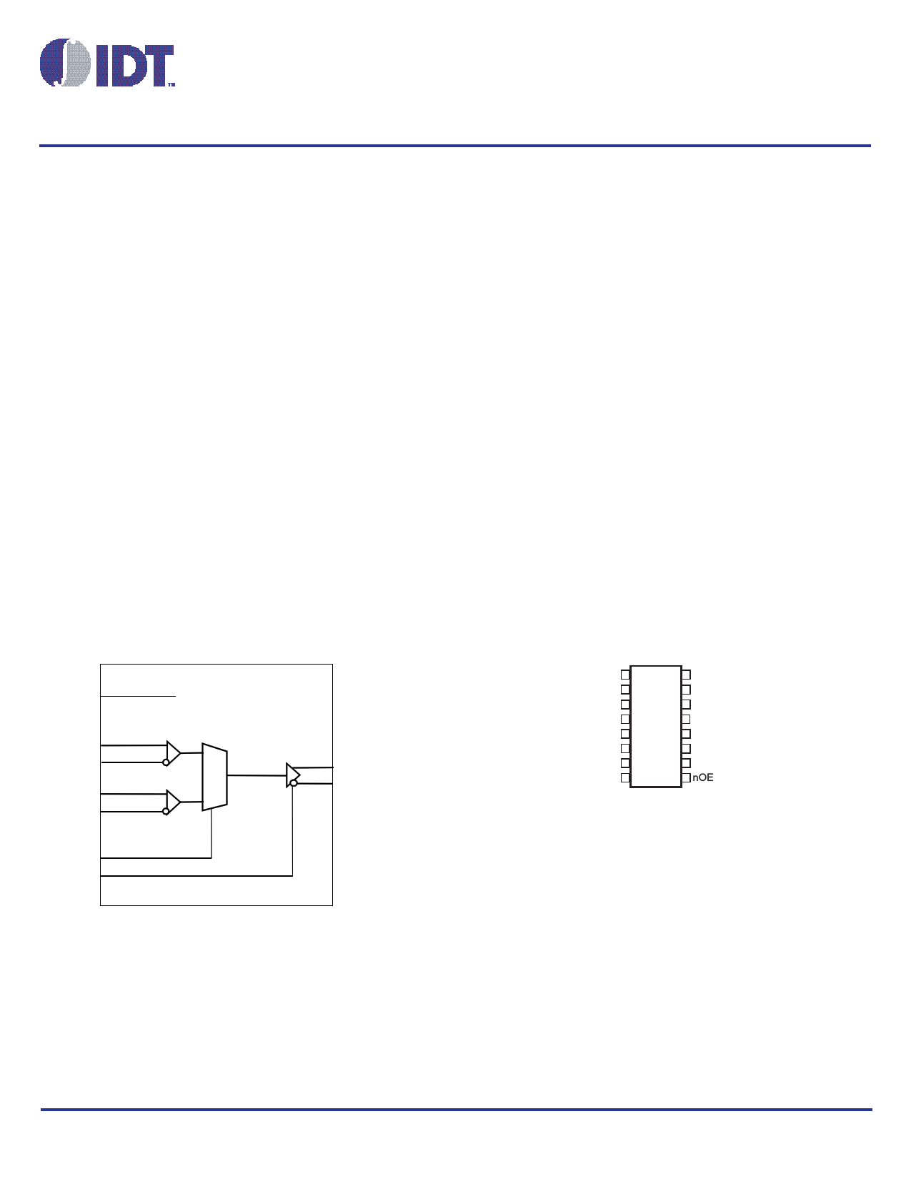
Block Diagram
IREF
CLK0 Pulldown
nCLK0 Pullup/down
CLK1 Pulldown
nCLK1 Pullup/down
SEL Pulldown
nOE Pullup
0
1
Q
nQ
Pin Assignment
CLK0
nCLK0
VDD
CLK1
nCLK1
GND
nc
VDD
1
2
3
4
5
6
7
8
16 IREF
15 SEL
14 VDD
13 nQ
12 Q
11 VDD
10 GND
9 nOE
ICS831721I
16 Lead TSSOP
4.4mm x 5.0mm x 0.925mm package body
G Package
Top View
ICS831721AGI REVISION A AUGUST 19, 2011
1
©2011 Integrated Device Technology, Inc.
1 page 
ICS831721I Data Sheet
DIFFERENTIAL CLOCK/DATA MULTIPLEXER
AC Electrical Characteristics
Table 5. HCSL AC Characteristics, VDD = 3.3V ± 0.3V, TA = -40°C to 85°C
Symbol
Parameter
Test Conditions
fOUT
tjit
Output Frequency
Buffer Additive Phase Jitter, RMS;
refer to Additive Phase Jitter Plot
100MHz, Integration Range:
12kHz – 20MHz
tPD
tsk(i)
Propagation Delay, NOTE 1
Input Skew; NOTE 2
Any CLKx, nCLKx to Q, nQ
tsk(pp)
Part-to-Part Skew;
NOTE 3, 4
Edge Rate Rise/Fall Edge Rate; NOTE 5, 6
VRB
VMAX
Ringback Voltage; NOTE 5, 7
Absolute Max Output Voltage; NOTE
8, 9
VMIN
Absolute Min Output Voltage; NOTE
8, 10
VCROSS
Absolute Crossing Voltage;
NOTE 8, 11, 12
∆VCROSS
Total Variation of VCROSS over all
edges; NOTE 8, 11, 13
odc
MUXISOL
Output Duty Cycle; NOTE 14
Mux Isolation; NOTE 15
fOUT < 312.5MHz
fOUT > 312.5MHz
ƒ = 100MHz
Minimum Typical
0.314
2
0.6
-100
Maximum
700
0.337
2.4
55
400
4.0
100
1150
Units
MHz
ps
ns
ps
ps
V/ns
V
mV
-300
mV
250 550 mV
140 mV
46
43
80
54 %
57 %
dB
NOTE: Electrical parameters are guaranteed over the specified ambient operating temperature range, which is established when the device is
mounted in a test socket with maintained transverse airflow greater than 500 lfpm. The device will meet specifications after thermal equilibrium
has been reached under these conditions.
NOTE 1: Measured from the differential input cross point to the differential output crossing point.
NOTE 2: Defined as skew between input paths on the same device, using the same input signal levels, measured at one specific output at the
differential cross points.
NOTE 3: This parameter is defined in accordance with JEDEC Standard 65.
NOTE 4: Defined as skew between outputs on different devices operating at the same supply voltage and with equal load conditions. Using
the same type of inputs on each device, the outputs are measured at the differential cross points.
NOTE 5: Measurement taken from differential waveform.
NOTE 6: Measurement from -150mV to +150mV on the differential waveform (derived from Q minus nQ). The signal must be monotonic
through the measurement region for rise and fall time. The 300mV measurement window is centered on the differential zero crossing.
NOTE 7: TSTABLE is the time the differential clock must maintain a minimum ±150mV differential voltage after rising/falling edges before it is
allowed to drop back into the VRB ±100 differential range. See Parameter Measurement Information Section.
NOTE 8: Measurement taken from single-ended waveform.
NOTE 9: Defined as the maximum instantaneous voltage including overshoot. See Parameter Measurement Information Section.
NOTE 10: Defined as the minimum instantaneous voltage including undershoot. See Parameter Measurement Information Section.
NOTE 11: Measured at crossing point where the instantaneous voltage value of the rising edge of Qx equals the falling edge of nQx.
See Parameter Measurement Information Section
NOTE 12: Refers to the total variation from the lowest crossing point to the highest, regardless of which edge is crossing. Refers to all crossing
points for this measurement. See Parameter Measurement Information Section.
NOTE 13: Defined as the total variation of all crossing voltage of rising Q and falling nQ. This is the maximum allowed variance in the VCROSS
for any particular system. See Parameter Measurement Information Section.
NOTE 14: Input duty cycle must be 50%.
NOTE 15: Q, nQ output measured differentially. See MUX Isolation Diagram in Parameter Measurement Information Section.
ICS831721AGI REVISION A AUGUST 19, 2011
5
©2011 Integrated Device Technology, Inc.
5 Page 
ICS831721I Data Sheet
DIFFERENTIAL CLOCK/DATA MULTIPLEXER
Recommended Termination
Figure 3A is the recommended source termination for applications
where the driver and receiver will be on a separate PCBs. This
termination is the standard for PCI Express™ and HCSL output
types. All traces should be 50Ω impedance single-ended or
100Ω differential.
0.5" Max
L1
Rs
22 to 33 +/-5%
0-0.2"
L2
PCI Express
D ri ve r
L1
L2
0-0.2" L3 L3
1-14"
L4
L4
PCI Expres s
C o n n e cto r
0.5 - 3.5"
L5
L5
PCI Express
Add-in Card
Rt 49.9 +/- 5%
Figure 3A. Recommended Source Termination (where the driver and receiver will be on separate PCBs)
Figure 3B is the recommended termination for applications where a
point-to-point connection can be used. A point-to-point connection
contains both the driver and the receiver on the same PCB. With a
matched termination at the receiver, transmission-line reflections will
be minimized. In addition, a series resistor (Rs) at the driver
offers flexibility and can help dampen unwanted reflections.
The optional resistor can range from 0Ω to 33Ω. All traces
should be 50Ω impedance single-ended or 100Ω differential.
0.5" Max
L1
L1
PCI Express
Driver
Rs
0 to 33
0 to 33
0-18"
L2
L2
Rt
0-0.2"
L3
L3
49.9 +/- 5%
Figure 3B. Recommended Termination (where a point-to-point connection can be used)
ICS831721AGI REVISION A AUGUST 19, 2011
11
©2011 Integrated Device Technology, Inc.
11 Page | ||
| Páginas | Total 17 Páginas | |
| PDF Descargar | [ Datasheet ICS831721I.PDF ] | |
Hoja de datos destacado
| Número de pieza | Descripción | Fabricantes |
| ICS831721I | Differential Clock/Data Multiplexer | IDT |
| Número de pieza | Descripción | Fabricantes |
| SLA6805M | High Voltage 3 phase Motor Driver IC. |
Sanken |
| SDC1742 | 12- and 14-Bit Hybrid Synchro / Resolver-to-Digital Converters. |
Analog Devices |
|
DataSheet.es es una pagina web que funciona como un repositorio de manuales o hoja de datos de muchos de los productos más populares, |
| DataSheet.es | 2020 | Privacy Policy | Contacto | Buscar |