|
|
|
PDF NVB5404N Data sheet ( Hoja de datos )
| Número de pieza | NVB5404N | |
| Descripción | Power MOSFET ( Transistor ) | |
| Fabricantes | ON Semiconductor | |
| Logotipo | ||
Hay una vista previa y un enlace de descarga de NVB5404N (archivo pdf) en la parte inferior de esta página. Total 7 Páginas | ||
|
No Preview Available !
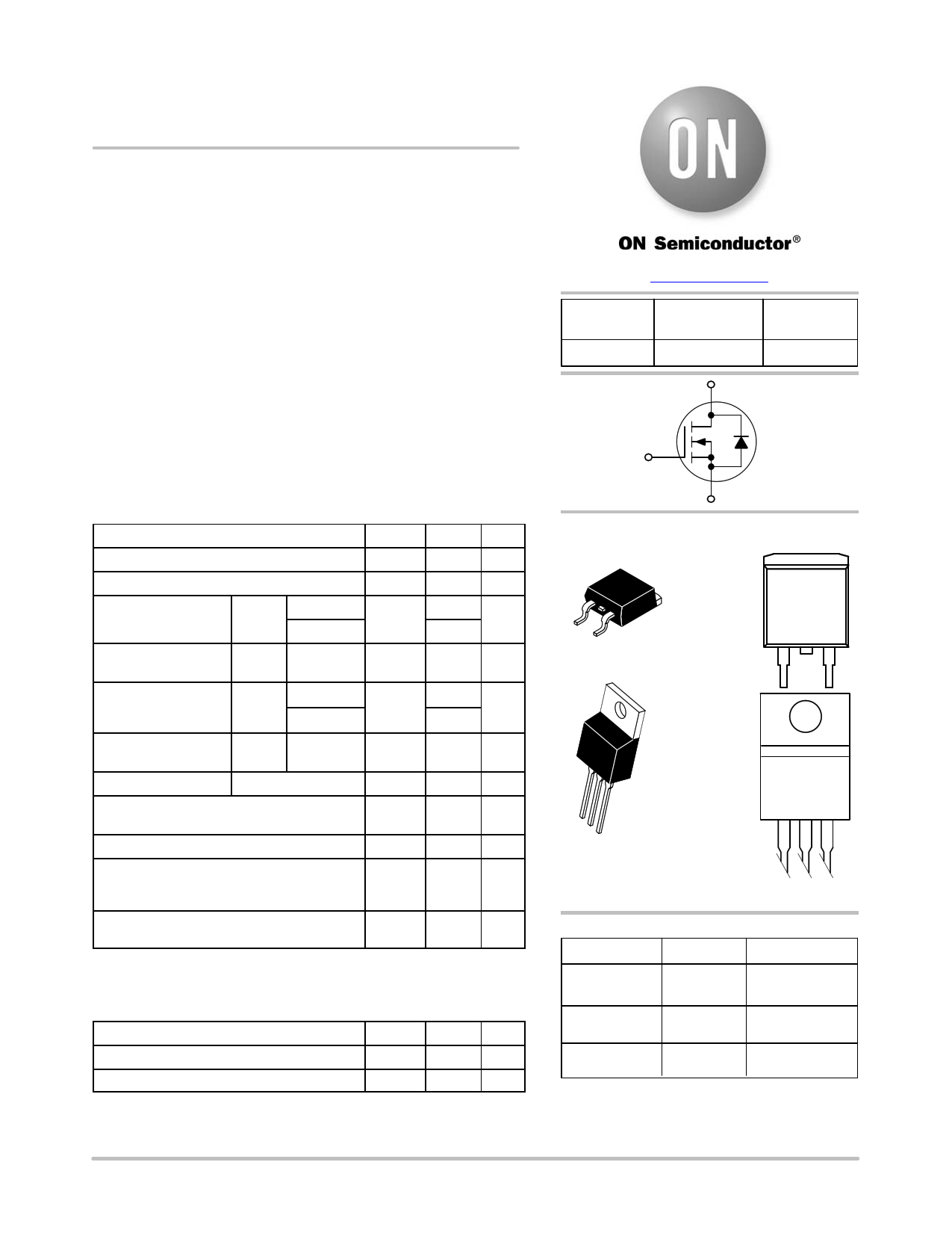
NTB5404N, NTP5404N,
NVB5404N
Power MOSFET
40 V, 167 A, Single N−Channel, D2PAK &
TO−220
Features
• Low RDS(on)
• High Current Capability
• Low Gate Charge
• AEC−Q101 Qualified and PPAP Capable − NVB5404N
• These Devices are Pb−Free and are RoHS Compliant
Applications
• Electronic Brake Systems
• Electronic Power Steering
• Bridge Circuits
MAXIMUM RATINGS (TJ = 25°C unless otherwise stated)
Parameter
Symbol Value Units
Drain−to−Source Voltage
VDSS 40 V
Gate−to−Source Voltage
VGS ±20 V
Continuous Drain
Current − RqJC
Steady TC = 25°C
State TC = 100°C
ID
167 A
118
Power Dissipation −
RqJC
Steady
State
TC = 25°C
PD
254 W
Continuous Drain
Current − RqJA
(Note 1)
Steady TA = 25°C
State
TA = 100°C
ID
24 A
17
Power Dissipation −
RqJA (Note 1)
Steady TA = 25°C
State
Pulsed Drain Current
tp = 10 ms
Operating Junction and Storage Temperature
PD
IDM
TJ,
TSTG
5.4 W
670
−55 to
175
A
°C
Source Current (Body Diode) Pulsed
Single Pulse Drain−to Source Avalanche
Energy − (VDD = 50 V, VGS = 10 V, IPK = 45 A,
L = 1 mH, RG = 25 W)
Lead Temperature for Soldering Purposes
(1/8” from case for 10 s)
IS
EAS
TL
75
1000
A
mJ
260 °C
Stresses exceeding those listed in the Maximum Ratings table may damage the
device. If any of these limits are exceeded, device functionality should not be
assumed, damage may occur and reliability may be affected.
THERMAL RESISTANCE RATINGS
Parameter
Symbol Max Unit
Junction−to−Case (Drain)
RθJC
Junction−to−Ambient (Note 1)
RθJA
1. Surface mounted on FR4 board using 1 sq in pad size,
(Cu Area 1.127 sq in [2 oz] including traces).
0.59 °C/W
50 °C/W
© Semiconductor Components Industries, LLC, 2015
January, 2015 − Rev. 8
1
www.onsemi.com
V(BR)DSS
40 V
RDS(ON) MAX
4.5 mW @ 10 V
D
ID MAX
(Note 1)
167 A
N−Channel
G
S
MARKING
DIAGRAMS
1
2
3
4
D2PAK
CASE 418B
STYLE 2
NTB5404NG
AYWW
1
TO−220AB
CASE 221A
STYLE 5
NTP5404NRG
AYWW
1
2
3G
A
Y
WW
= Pb−Free Device
= Assembly Location
= Year
= Work Week
ORDERING INFORMATION
Device
Package
Shipping†
NTB5404NT4G
D2PAK 800 / Tape & Reel
(Pb−Free)
NTP5404NRG
NVB5404NT4G
TO−220
(Pb−Free)
D2PAK
(Pb−Free)
50 Units / Rail
800 / Tape & Reel
†For information on tape and reel specifications,
including part orientation and tape sizes, please
refer to our Tape and Reel Packaging Specifications
Brochure, BRD8011/D.
Publication Order Number:
NTB5404N/D
1 page 
100
50% Duty Cycle
10
20%
10%
5%
2%
1 1%
0.1
0.01
SINGLE PULSE
0.001
0.000001 0.00001
NTB5404N, NTP5404N, NVB5404N
0.0001
P(pk)
RqJA(t) = r(t) RqJA
D CURVES APPLY FOR POWER
PULSE TRAIN SHOWN
t1 READ TIME AT t1
t2 TJ(pk) − TC = P(pk) RqJA(t)
DUTY CYCLE, D = t1/t2
0.001
0.01
0.1
1
10 100 1000
t, PULSE TIME (sec)
Figure 12. Thermal Response
www.onsemi.com
5
5 Page | ||
| Páginas | Total 7 Páginas | |
| PDF Descargar | [ Datasheet NVB5404N.PDF ] | |
Hoja de datos destacado
| Número de pieza | Descripción | Fabricantes |
| NVB5404N | Power MOSFET ( Transistor ) | ON Semiconductor |
| NVB5404NT4G | Power MOSFET ( Transistor ) | ON Semiconductor |
| Número de pieza | Descripción | Fabricantes |
| SLA6805M | High Voltage 3 phase Motor Driver IC. |
Sanken |
| SDC1742 | 12- and 14-Bit Hybrid Synchro / Resolver-to-Digital Converters. |
Analog Devices |
|
DataSheet.es es una pagina web que funciona como un repositorio de manuales o hoja de datos de muchos de los productos más populares, |
| DataSheet.es | 2020 | Privacy Policy | Contacto | Buscar |