|
|
|
PDF FDS4895C Data sheet ( Hoja de datos )
| Número de pieza | FDS4895C | |
| Descripción | Dual N & P-Channel PowerTrench MOSFET | |
| Fabricantes | Fairchild Semiconductor | |
| Logotipo | ||
Hay una vista previa y un enlace de descarga de FDS4895C (archivo pdf) en la parte inferior de esta página. Total 8 Páginas | ||
|
No Preview Available !
www.DataSheet4U.com
June 2005
FDS4895C
Dual N & P-Channel PowerTrench® MOSFET
General Description
These dual N- and P-Channel enhancement mode
power field effect transistors are produced using
Fairchild Semiconductor’s advanced PowerTrench
process that has been especially tailored to minimize
on-state resistance and yet maintain superior switching
performance.
Application
• Motor Control
• DC/DC conversion
Features
• Q1: N-Channel
5.5A, 40V RDS(on) = 39mΩ @ VGS = 10V
RDS(on) = 57mΩ @ VGS = 7V
• Q2: P-Channel
–4.4A, –40V RDS(on) = 46mΩ @ VGS = –10V
RDS(on) = 63mΩ @ VGS = –4.5V
• High power and handling capability in a widely
used surface mount package
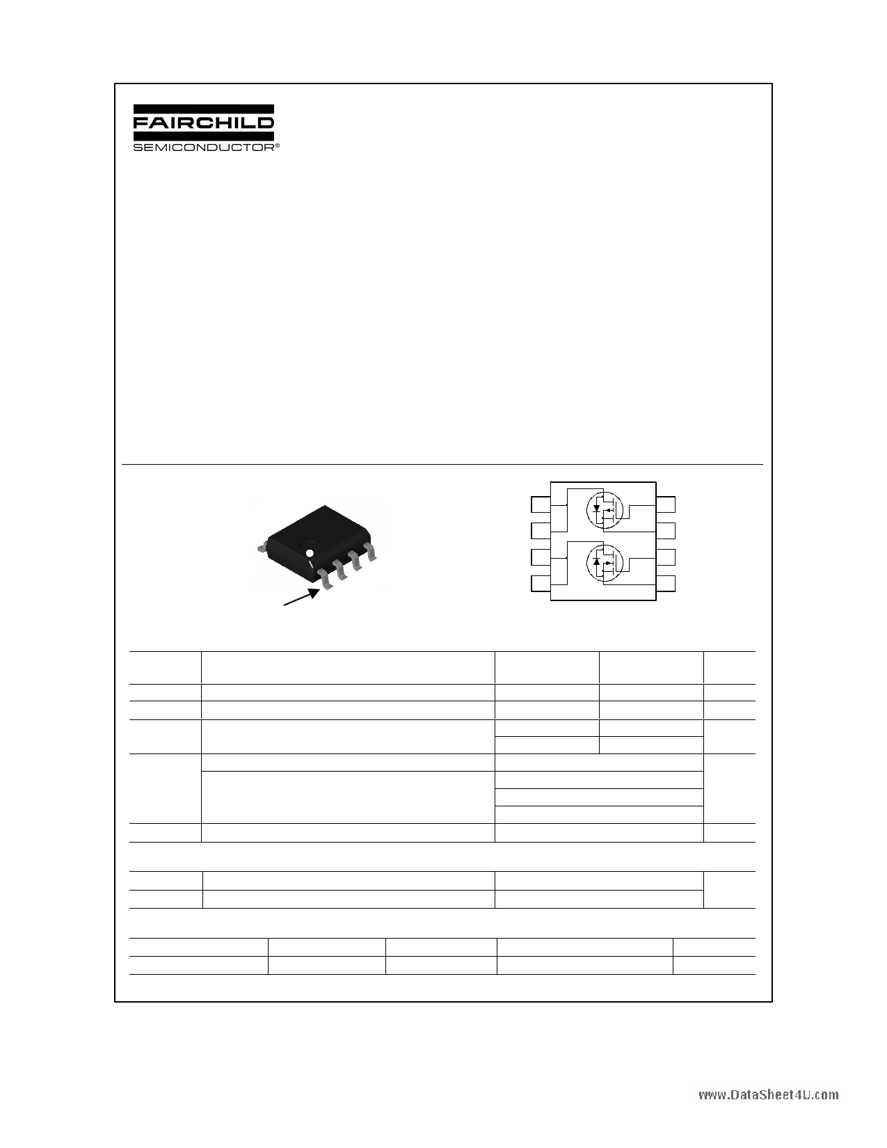
DD2DD2
DD1
DD1
SO-8
Pin 1 SO-8
G2
S2 G
G1
S1 S
S
S
Absolute Maximum Ratings TA = 25°C unless otherwise noted
Symbol
VDSS
VGSS
ID
PD
TJ, TSTG
Parameter
Drain-Source Voltage
Gate-Source Voltage
Drain Current - Continuous
(Note 1a)
- Pulsed
Power Dissipation for Dual Operation
Power Dissipation for Single Operation
(Note 1a)
(Note 1b)
(Note 1c)
Operating and Storage Junction Temperature Range
Thermal Characteristics
RθJA Thermal Resistance, Junction-to-Ambient
RθJC Thermal Resistance, Junction-to-Case
(Note 1a)
(Note 1)
Package Marking and Ordering Information
Device Marking
Device
Reel Size
FDS4895C
FDS4895C
13”
Q2
5
6
Q1
7
8
4
3
2
1
Q1 Q2
40 40
±20 ±20
5.5 –4.4
20 –20
2
1.6
1
0.9
–55 to +150
78
40
Units
V
V
A
W
°C
°C/W
Tape width
12mm
Quantity
2500 units
©2005 Fairchild Semiconductor Corporation
FDS4895C Rev C(W)
1 page 
www.DataSheet4U.com
Typical Characteristics: Q1 (N-Channel)
14
ID = 5.5A
12
10
8
6
4
2
0
02
VDS = 10V
20V
30V
4 6 8 10 12
Qg, GATE CHARGE (nC)
Figure 7. Gate Charge Characteristics.
100
RDS(ON) LIMIT
10
1
100 µs
1ms
10ms
100ms
1s
10s
DC
0.1 VGS = 10.0V
SINGLE PULSE
RθJA = 135oC/W
TA = 25oC
0.01
0.1 1 10
VDS, DRAIN-SOURCE VOLTAGE (V)
100
Figure 9. Maximum Safe Operating Area.
600
f = 1 MHz
VGS = 0 V
500
C iss
400
300
200
100
Crss
0
0
5
C oss
10 15 20 25 30
VDS, DRAIN TO SOURCE VOLTAGE (V)
35
40
Figure 8. Capacitance Characteristics.
50
SINGLE PULSE
40
RθJA = 135°C/W
TA = 25°C
30
20
10
0
0.001
0.01
0.1 1 10
t1, TIME (sec)
100
Figure 10. Single Pulse Maximum
Power Dissipation.
1000
FDS4895C Rev C(W)
5 Page | ||
| Páginas | Total 8 Páginas | |
| PDF Descargar | [ Datasheet FDS4895C.PDF ] | |
Hoja de datos destacado
| Número de pieza | Descripción | Fabricantes |
| FDS4895C | Dual N & P-Channel PowerTrench MOSFET | Fairchild Semiconductor |
| Número de pieza | Descripción | Fabricantes |
| SLA6805M | High Voltage 3 phase Motor Driver IC. |
Sanken |
| SDC1742 | 12- and 14-Bit Hybrid Synchro / Resolver-to-Digital Converters. |
Analog Devices |
|
DataSheet.es es una pagina web que funciona como un repositorio de manuales o hoja de datos de muchos de los productos más populares, |
| DataSheet.es | 2020 | Privacy Policy | Contacto | Buscar |