|
|
|
PDF STP12NK60Z Data sheet ( Hoja de datos )
| Número de pieza | STP12NK60Z | |
| Descripción | N-CHANNEL MOSFET | |
| Fabricantes | STMicroelectronics | |
| Logotipo | ||
Hay una vista previa y un enlace de descarga de STP12NK60Z (archivo pdf) en la parte inferior de esta página. Total 15 Páginas | ||
|
No Preview Available !
STP12NK60Z
STF12NK60Z, STW12NK60Z
N-channel 650 V @Tjmax, 0.53 Ω, 10 A TO-220, TO-220FP, TO-247
Zener-protected SuperMESH™ Power MOSFET
Features
Type
VDSS
RDS(on)
(@Tjmax) max
ID
PW
STP12NK60Z
STF12NK60Z
STW12NK60Z
650 V
650 V
650 V
<0.640 Ω 10 A 150 W
<0.640 Ω 10 A 35 W
<0.640 Ω 10 A 150 W
■ Extremely high dv/dt capability
■ 100% avalanche tested
■ Gate charge minimized
■ Very low intrinsic capacitances
■ Very good manufacturing repeatability
Application
■ Switching applications
Description
The SuperMESH™ series is obtained through an
extreme optimization of ST’s well established
strip-based PowerMESH™ layout. In addition to
pushing on-resistance significantly down,
specialties is taken to ensure a very good dv/dt
capability for the most demanding application.
Such series complements ST full range of high
voltage Power MOSFETs.
Table 1. Device summary
Order codes
Marking
STP12NK60Z
STF12NK60Z
STW12NK60Z
P12NK60Z
F12NK60Z
W12NK60Z
3
2
1
TO-220FP
3
2
1
TO-220
3
2
1
TO-247
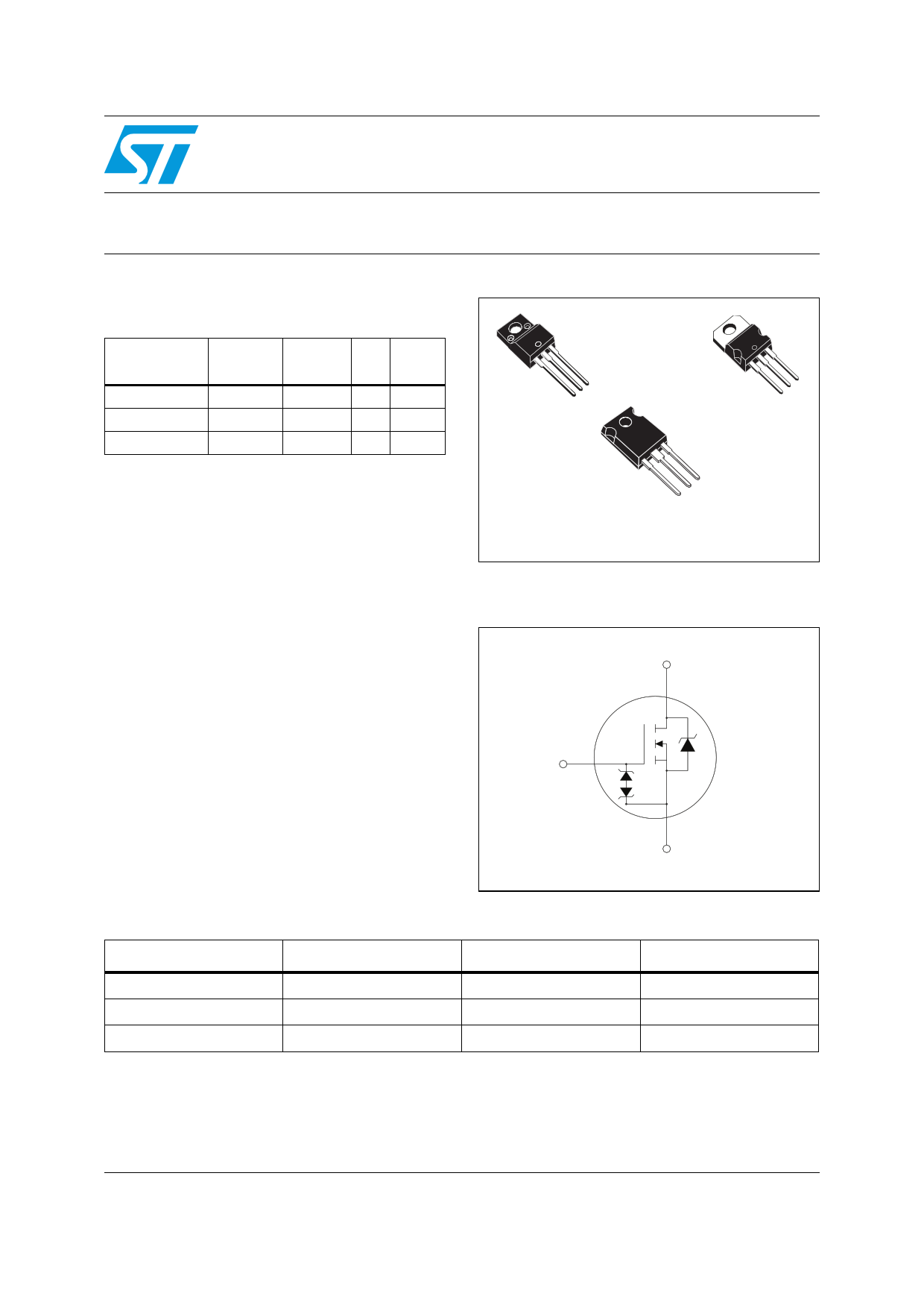
Figure 1. Internal schematic diagram
D(2)
G(1)
Package
TO-220
TO-220FP
TO-247
S(3)
AM01476v1
Packaging
Tube
Tube
Tube
October 2009
Doc ID 11324 Rev 7
1/15
www.st.com
15
1 page 
STP12NK60Z, STF12NK60Z, STW12NK60Z
Electrical characteristics
Table 7. Source drain diode
Symbol
Parameter
Test conditions
Min Typ. Max Unit
ISD
ISDM (1)
VSD (2)
Source-drain current
Source-drain current (pulsed)
Forward on voltage
ISD = 10 A, VGS = 0
trr
Qrr
IRRM
Reverse recovery time
Reverse recovery charge
Reverse recovery current
ISD = 10 A, di/dt = 100 A/µs
VDD = 50 V
(see Figure 24)
trr
Qrr
IRRM
Reverse recovery time
Reverse recovery charge
Reverse recovery current
ISD = 10 A, di/dt = 100 A/µs
VDD = 50 V, Tj = 150 °C
(see Figure 24)
1. Pulse width limited by safe operating area
2. Pulsed: Pulse duration = 300 µs, duty cycle 1.5%
10 A
-
40 A
- 1.6 V
358
-3
17
ns
µC
A
460
- 4.2
18.2
ns
µC
A
Table 8.
Symbol
Gate-source Zener diode
Parameter
Test conditions
Min Typ Max Unit
BVGSO (1)
Gate-Source breakdown
voltage
Igs=± 1 mA (open drain)
30 - - V
1. The built-in back-to-back Zener diodes have specifically been designed to enhance not only the device’s
ESD capability, but also to make them safely absorb possible voltage transients that may occasionally be
applied from gate to source. In this respect the Zener voltage is appropriate to achieve an efficient and
cost-effective intervention to protect the device’s integrity. These integrated Zener diodes thus avoid the
usage of external components.
Doc ID 11324 Rev 7
5/15
5 Page 
STP12NK60Z, STF12NK60Z, STW12NK60Z
Package mechanical data
TO-220 type A mechanical data
mm
Dim
Min Typ
A 4.40
b 0.61
b1 1.14
c 0.48
D 15.25
D1 1.27
E 10
e 2.40
e1 4.95
F 1.23
H1 6.20
J1 2.40
L 13
L1 3.50
L20 16.40
L30 28.90
∅P 3.75
Q 2.65
Max
4.60
0.88
1.70
0.70
15.75
10.40
2.70
5.15
1.32
6.60
2.72
14
3.93
3.85
2.95
Doc ID 11324 Rev 7
0015988_Rev_S
11/15
11 Page | ||
| Páginas | Total 15 Páginas | |
| PDF Descargar | [ Datasheet STP12NK60Z.PDF ] | |
Hoja de datos destacado
| Número de pieza | Descripción | Fabricantes |
| STP12NK60Z | N-CHANNEL MOSFET | STMicroelectronics |
| Número de pieza | Descripción | Fabricantes |
| SLA6805M | High Voltage 3 phase Motor Driver IC. |
Sanken |
| SDC1742 | 12- and 14-Bit Hybrid Synchro / Resolver-to-Digital Converters. |
Analog Devices |
|
DataSheet.es es una pagina web que funciona como un repositorio de manuales o hoja de datos de muchos de los productos más populares, |
| DataSheet.es | 2020 | Privacy Policy | Contacto | Buscar |