|
|
|
PDF BUZ11 Data sheet ( Hoja de datos )
| Número de pieza | BUZ11 | |
| Descripción | N-Channel Power MOSFET / Transistor | |
| Fabricantes | Fairchild Semiconductor | |
| Logotipo | ||
 1. - 50V, 30A, N-Channel MOSFET Hay una vista previa y un enlace de descarga de BUZ11 (archivo pdf) en la parte inferior de esta página. Total 6 Páginas | ||
|
No Preview Available !
Data Sheet
BUZ11
September 2013 File Number 2253.2
N-Channel Power MOSFET
50V, 30A, 40 mΩ
This is an N-Channel enhancement mode silicon gate power
field effect transistor designed for applications such as
switching regulators, switching converters, motor drivers,
relay drivers and drivers for high power bipolar switching
transistors requiring high speed and low gate drive power.
This type can be operated directly from integrated circuits.
Formerly developmental type TA9771.
Ordering Information
PART NUMBER
PACKAGE
BRAND
BUZ11_NR4941 TO-220AB
BUZ11
NOTE: When ordering, use the entire part number.
Features
• 30A, 50V
• rDS(ON) = 0.040Ω
• SOA is Power Dissipation Limited
• Nanosecond Switching Speeds
• Linear Transfer Characteristics
• High Input Impedance
• Majority Carrier Device
• Related Literature
- TB334 “Guidelines for Soldering Surface Mount
Components to PC Boards”
Symbol
D
G
S
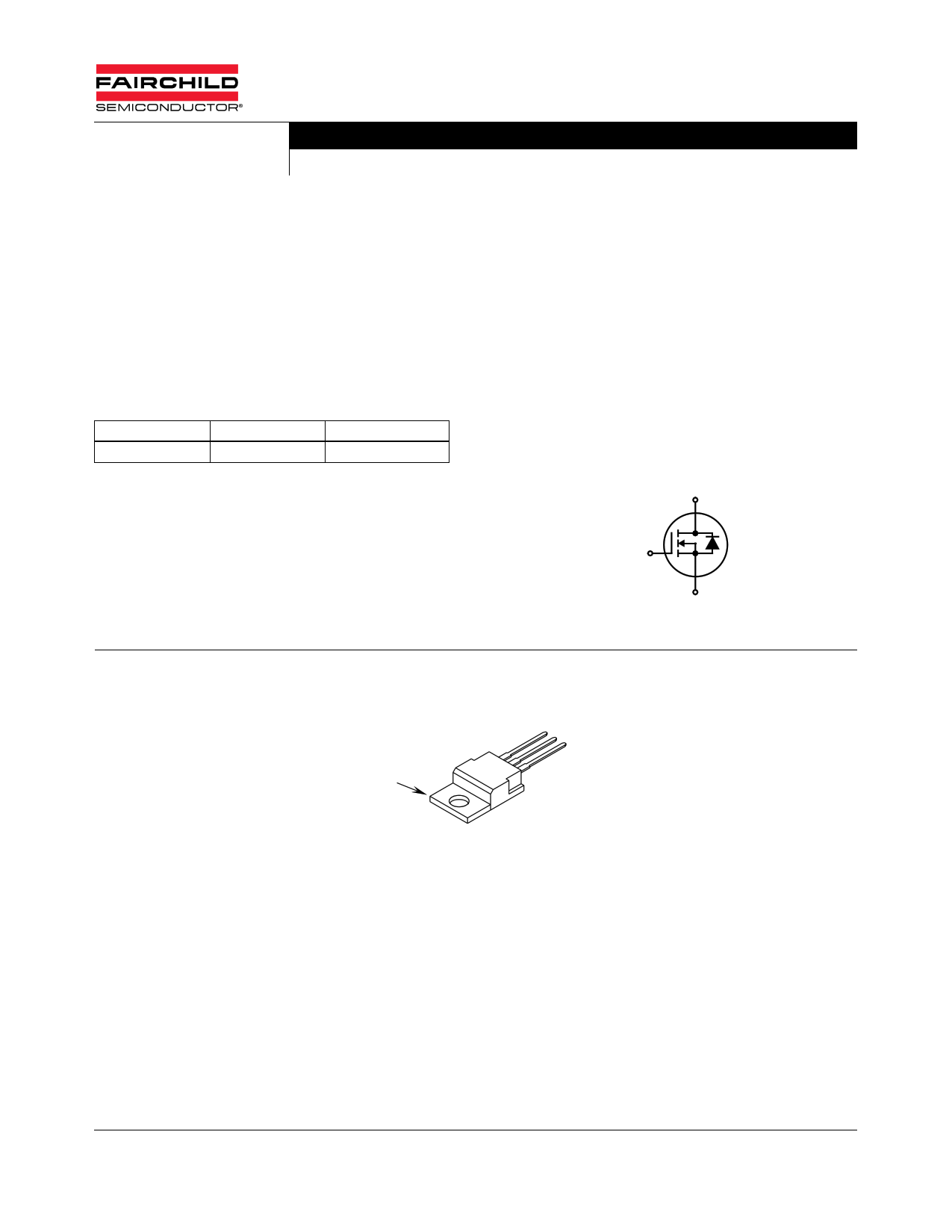
Packaging
JEDEC TO-220AB
DRAIN (FLANGE)
SOURCE
DRAIN
GATE
©2001 Fairchild Semiconductor Corporation
BUZ11 Rev. C0
1 page 
BUZ11
Typical Performance Curves Unless Otherwise Specified (Continued)
103 PULSE DURATION = 80µs
DUTY CYCLE = 0.5% MAX
102
TJ = 25oC
TJ = 150oC
15
ID = 45A
10
101
5
100
VDS = 10V
VDS = 40V
10-1
0
0.5 1.0 1.5 2.0 2.5
VSD, SOURCE TO DRAIN VOLTAGE (V)
3.0
FIGURE 12. SOURCE TO DRAIN DIODE VOLTAGE
0
0 10 20 30 40 50
Qg, GATE CHARGE (nC)
FIGURE 13. GATE TO SOURCE VOLTAGE vs GATE CHARGE
Test Circuits and Waveforms
RL
+
RG
VDD
-
DUT
VGS
FIGURE 14. SWITCHING TIME TEST CIRCUIT
CURRENT
REGULATOR
VDS
(ISOLATED
SUPPLY)
12V
BATTERY
0.2µF 50kΩ
0.3µF
SAME TYPE
AS DUT
D
G DUT
Ig(REF)
0
S
VDS
IG CURRENT
SAMPLING
ID CURRENT
SAMPLING
RESISTOR
RESISTOR
FIGURE 16. GATE CHARGE TEST CIRCUIT
VDS
tON
td(ON)
tr
90%
tOFF
td(OFF)
tf
90%
10%
0
VGS
10%
0
50%
PULSE WIDTH
10%
90%
50%
FIGURE 15. RESISTIVE SWITCHING WAVEFORMS
VDD
Qgs
Qg(TOT)
Qgd
VGS
VDS
0
Ig(REF)
0
FIGURE 17. GATE CHARGE WAVEFORMS
©2001 Fairchild Semiconductor Corporation
BUZ11 Rev. C0
5 Page | ||
| Páginas | Total 6 Páginas | |
| PDF Descargar | [ Datasheet BUZ11.PDF ] | |
Hoja de datos destacado
| Número de pieza | Descripción | Fabricantes |
| BUZ10 | N - CHANNEL 50V - 0.06W - 23A TO-220 STripFET] MOSFET | STMicroelectronics |
| BUZ10 | SIPMOS Power Transistor (N channel Enhancement mode Avalanche-rated) | Siemens Semiconductor Group |
| BUZ10 | Trans MOSFET N-CH 50V 23A 3-Pin(3+Tab) TO-220 | New Jersey Semiconductor |
| BUZ100 | SIPMOS Power Transistor (N channel Enhancement mode Avalanche-rated d v/d t rated) | Siemens Semiconductor Group |
| Número de pieza | Descripción | Fabricantes |
| SLA6805M | High Voltage 3 phase Motor Driver IC. |
Sanken |
| SDC1742 | 12- and 14-Bit Hybrid Synchro / Resolver-to-Digital Converters. |
Analog Devices |
|
DataSheet.es es una pagina web que funciona como un repositorio de manuales o hoja de datos de muchos de los productos más populares, |
| DataSheet.es | 2020 | Privacy Policy | Contacto | Buscar |