|
|
|
PDF IS31BL3233A Data sheet ( Hoja de datos )
| Número de pieza | IS31BL3233A | |
| Descripción | 1.5A FLASH/TORCH LED DRIVER | |
| Fabricantes | ISSI | |
| Logotipo | ||
Hay una vista previa y un enlace de descarga de IS31BL3233A (archivo pdf) en la parte inferior de esta página. Total 13 Páginas | ||
|
No Preview Available !
IS31BL3233A
2MHz, 1.5A FLASH/TORCH LED DRIVER
Preliminary Information
September 2014
GENERAL DESCRIPTION
The IS31BL3233A is the ideal power solution for
high-power flash LEDs used with cell phone camera
modules or digital still cameras. It is a highly integrated
step up DC-DC converter with very high switching
frequency, fixed at 2MHz, providing a very small total
solution for portable photo flash. The IS31BL3233A has
separate Flash Mode and Torch Mode enable pins for
maximum flexibility. The Flash Mode and Torch Mode
LED current is programmed by external resistors
respectively, making the flash LED solution simple to
control. If both enable pins are at logic high, the LED
current will be programmed by the Torch Mode setting
resistor. The two LED output sinks can be shorted
together externally for higher power single flash LEDs,
up to 1.5A continuous LED current. Thermal regulation
is integrated in Flash Mode to limit the IC’s temperature
and continuously provide the maximum allowed output
current.
Various protection features are built into the
IS31BL3233A, including cycle-by-cycle input current
limit protection, output over-voltage protection, LED
fault (open or short) protection and thermal shutdown
protection. The IS31BL3233A is available in a RoHS
compliant DFN-14 (2mm × 3mm) package.
FEATURES
Input voltage range: 2.7V~5.5V
Dual flash LED outputs
Drive up to total 1.5A or 0.75A per channel
1s time out in Flash Mode to protect LED
High efficiency up to 93% (1A, Flash Mode)
2MHz step-up converter
Independent Flash Mode enable and Torch Mode
enable pins
Torch Mode dimming via PWM control
Integrated thermal regulation control
LED open/short protection
Over-voltage protection
Cycle-by-cycle inductor current limit
Pb-free package: DFN-14 (2mm×3mm)
-40C° ~ +85C° temperature range
APPLICATIONS
Mobile phones
Smart phones and PDAs
Digital still cameras
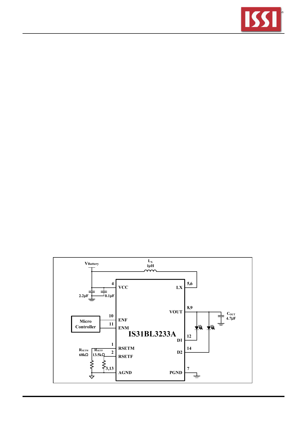
TYPICAL APPLICATION CIRCUIT
Figure 1 Typical Application Circuit (Torch Mode current is100mA and Flash Mode current is 500mA)
Integrated Silicon Solution, Inc. – www.issi.com
Rev. 0C, 09/11/2014
1
1 page 
IS31BL3233A
ABSOLUTE MAXIMUM RATINGS
Supply voltage, VCC
Voltage at any input pin
Maximum junction temperature, TJMAX
Storage temperature range, TSTG
Operating temperature range, TA
ESD (HBM)
ESD (CDM)
-0.3V ~ +6.0V
-0.3V ~ VCC+0.3V
150°C
-65°C ~ +150°C
−40°C ~ +85°C
8kV
1kV
Note:
Stresses beyond those listed under “Absolute Maximum Ratings” may cause permanent damage to the device. These are stress ratings only and
functional operation of the device at these or any other condition beyond those indicated in the operational sections of the specifications is not
implied. Exposure to absolute maximum rating conditions for extended periods may affect device reliability.
ELECTRICAL CHARACTERISTICS
The following specifications apply for VCC = 3.6V, TA = 25°C, unless otherwise noted.
Symbol
Description
Condition
Min.
Typ. Max. Units
IC Supply
VCC
UVLO
UVLOHYST
Input operating range
Input under voltage lockout
UVLO hysteresis
ICC Operating current
ISD Shutdown current
Step-Up Converter
ILIM
fSW
DMAX
VOVP
tS
Peak NMOS current limit
Oscillator frequency
Maximum duty cycle
Internal over voltage
threshold of VOUT
Flash mode soft start time
Current Sink
Total output current, Torch
Mode
IOUT Total output current, Flash
Mode
∆IOUT
Output current matching
(Note 2)
ISHORT
LED short checking
current
Rising edge
Not switching (RSETM = 135kΩ)
Switching (RSETM = 135kΩ)
VENF = VENM = GND
RSETF = 9.1kΩ (Note 1)
VENM = VCC, RSETM = 135kΩ,
D1+D2
VENF = VCC = 3.8V, VENM = GND,
RSETF = 9.1kΩ, D1+D2
50mA/CH
750m/CH
2.7 5.5 V
2.1 2.4 2.68 V
0.2 V
1.0 1.5 mA
1.8 2.6 mA
0.1 1 µA
3A
2.0 MHz
75 %
5.3 V
100 µs
90 100 110 mA
1.305 1.5 1.695 A
2 10 %
2 10 %
3.5 mA
Integrated Silicon Solution, Inc. – www.issi.com
Rev. 0C, 09/11/2014
5
5 Page 
IS31BL3233A
LED SHORT PROTECTION
When the IS31BL3233A is enabled, there is a 2.5mA
(Typ.) LED sensing current through each current sink. It
is used to detect whether either LED is shorted by
generating a voltage drop through each LED. The IC
internally compares the voltage difference between
VOUT and each sink node (D1 and D2). If this
difference is below a preset threshold (Typ. 1.7V), the
IC will treat the respective LED as shorted and disable
its Flash/Torch Mode current through this LED channel.
However, the 2.5mA sensing current will be kept to
generate the LED’s voltage drop. If the short circuit is
removed during operation, the channel will
automatically recover to the programmed current
setting.
LED OPEN PROTECTION
In case of LED open, the open channel will control the
loop first so that VOUT will reach OVP, then
IS31BL3233A will automatically detect which channel’s
LED is open and disable that channel. From that point,
the other channel with properly operating LED will
control the loop and VOUT will be regulated down to a
normal operating voltage. This protection feature
avoids unnecessary power consumption in the current
sink by regulating the output voltage at the lowest level
possible to maintain regulation for the active channel.
Not only does this protect from open LEDs failures, but
also allows only single flash LED operation with the
unused channel floating or open. Open-circuit LED fault
protection is reset when the IC is powered down and up
again.
INDUCTOR SELECTION
The IS31BL3233A is designed to use a 1.0μH to
4.7μH inductor. To prevent core saturation, ensure that
the inductor-saturation current rating exceeds the peak
inductor current for the application. The worst-case
peak inductor current can be calculated with the
following formula:
I PEAK( L)
V IOUT(MAX) LED(MAX)
0.8 VIN(MIN)
VIN(MIN) tON(MAX)
2L
where 0.8 is the estimated efficiency of 80%.
(3)
For example, for a 1.0A total (or 0.5A per channel) LED
current, the peak inductor current for a 1.0uH inductor
could be as high as (estimated 50% as the maximum
duty ratio at the minimum input voltage, maximum LED
forward voltage and maximum load current conditions):
I PEAK(L)
4V 1A
0.8 3.5V
3.5V 0.25
21
1.9 A
If the inductor value is smaller, the inductor peak
current will increase. To maintain stable operations for
the boost converter, the inductor peak current must be
less than both the IS31BL3233A current limit threshold
and the inductor saturation current rating.
Manufacturer’s specifications of inductors list both the
inductor DC current rating, which is a thermal limitation,
and peak inductor current rating, which is determined
by the saturation characteristics. Measurements at full
load and high ambient temperature should be
performed to ensure that the inductor does not saturate
or overheat due to its parasitic resistance. Bench
measurements are recommended to confirm actual
inductor peak current IPEAK and to ensure that the
inductor does not saturate at maximum LED current
and minimum input supply voltage.
CAPACITOR SELECTION
For good input voltage filtering low ESR ceramic
capacitors are recommended. At least a 2.2μF input
capacitor is recommended for high current flash LEDs
to improve transient behavior of the regulator and EMI
behavior of the total power supply circuit. The input
capacitor should be placed as close as possible to the
input pin and the PGND pin of the IS31BL3233A.
The output capacitance required depends on the
required LED current. A 4.7μF ceramic capacitor works
well in most situations, but a 1.0μF capacitor is
acceptable for lower LED current conditions.
PCB LAYOUT
Due to the fast switching transitions and high-current
paths, careful PC board layout is required. Connect
AGND pin directly to the exposed paddle underneath
the IC; connect the exposed paddle to the PCB ground
plane. The output bypass capacitor should be placed
as close to the IC as possible. Minimize trace lengths
between the IC and the inductor, the input capacitor,
and the output capacitor; keep these traces short,
direct, and wide. The ground connections of CIN and
COUT should be as close together as possible and
connected to PGND.
Integrated Silicon Solution, Inc. – www.issi.com
Rev. 0C, 09/11/2014
11
11 Page | ||
| Páginas | Total 13 Páginas | |
| PDF Descargar | [ Datasheet IS31BL3233A.PDF ] | |
Hoja de datos destacado
| Número de pieza | Descripción | Fabricantes |
| IS31BL3233A | 1.5A FLASH/TORCH LED DRIVER | ISSI |
| Número de pieza | Descripción | Fabricantes |
| SLA6805M | High Voltage 3 phase Motor Driver IC. |
Sanken |
| SDC1742 | 12- and 14-Bit Hybrid Synchro / Resolver-to-Digital Converters. |
Analog Devices |
|
DataSheet.es es una pagina web que funciona como un repositorio de manuales o hoja de datos de muchos de los productos más populares, |
| DataSheet.es | 2020 | Privacy Policy | Contacto | Buscar |