|
|
|
PDF 74HC05 Data sheet ( Hoja de datos )
| Número de pieza | 74HC05 | |
| Descripción | HEX INVERTER (OPEN DRAIN) | |
| Fabricantes | Toshiba | |
| Logotipo | ||
Hay una vista previa y un enlace de descarga de 74HC05 (archivo pdf) en la parte inferior de esta página. Total 7 Páginas | ||
|
No Preview Available !
TC74HC05AP/AF
TOSHIBA CMOS Digital Integrated Circuit Silicon Monolithic
TC74HC05AP, TC74HC05AF
Hex Inverter (open drain)
The TC74HC05A is a high speed CMOS INVERTER fabricated
with silicon gate C2MOS technology.
It achieves the high speed operation similar to equivalent
LSTTL while maintaining the CMOS low power dissipation.
Pin configuration and function are the same as the
TC74HC04A, but the TC74HC05A has high performance MOS
N-channel transistor (open-drain) outputs.
This device can, therefore, with a suitable pull-up resistors, be
used in wired-AND, LED drive and other applications.
All inputs are equipped with protection circuits against static
discharge or transient excess voltage.
Features
• High speed: tpz = 8 ns (typ.) at VCC = 5 V
• Low power dissipation: ICC = 1 μA (max) at Ta = 25°C
• High noise immunity: VNIH = VNIL = 28% VCC (min)
• Output drive capability: 10 LSTTL loads
• Wide operating voltage range: VCC (opr) = 2 to 6 V
• Open drain structure.
• Pin and function compatible with 74LS05
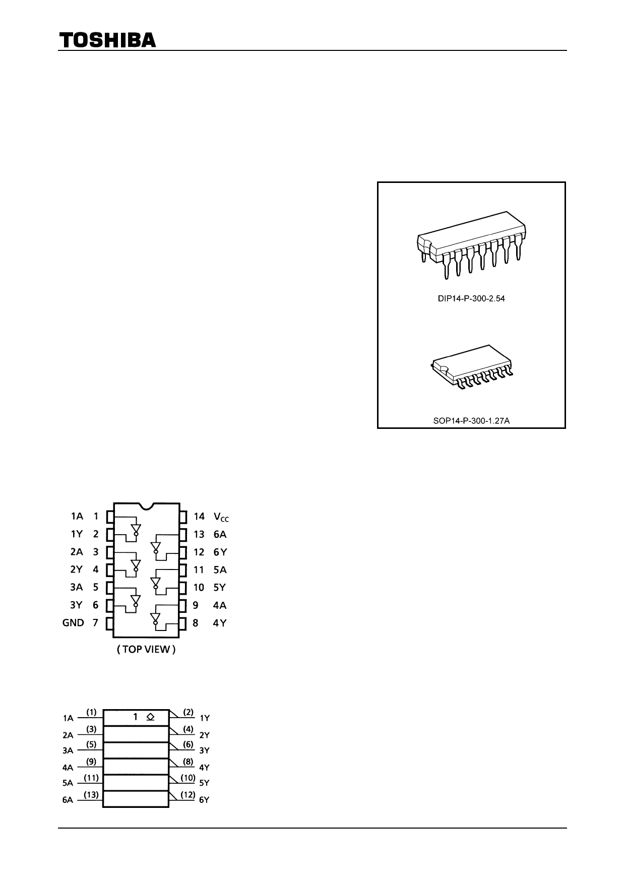
Pin Assignment
TC74HC05AP
TC74HC05AF
Weight
DIP14-P-300-2.54
SOP14-P-300-1.27A
: 0.96 g (typ.)
: 0.18 g (typ.)
IEC Logic Symbol
Start of commercial production
1988-05
1 2014-03-01
1 page 
Package Dimensions
TC74HC05AP/AF
Weight: 0.96 g (typ.)
5 2014-03-01
5 Page | ||
| Páginas | Total 7 Páginas | |
| PDF Descargar | [ Datasheet 74HC05.PDF ] | |
Hoja de datos destacado
| Número de pieza | Descripción | Fabricantes |
| 74HC00 | Quad 2-input NAND gate | Philips |
| 74HC00 | QUADRUPLE 2-INPUT NAND GATES | Diodes |
| 74HC00 | Quad 2-input NAND gate | NXP Semiconductors |
| 74HC01 | Quad. 2-input NAND Gates (with open drain outputs) | Hitachi |
| Número de pieza | Descripción | Fabricantes |
| SLA6805M | High Voltage 3 phase Motor Driver IC. |
Sanken |
| SDC1742 | 12- and 14-Bit Hybrid Synchro / Resolver-to-Digital Converters. |
Analog Devices |
|
DataSheet.es es una pagina web que funciona como un repositorio de manuales o hoja de datos de muchos de los productos más populares, |
| DataSheet.es | 2020 | Privacy Policy | Contacto | Buscar |