|
|
PDF 74ALVC32M Data sheet ( Hoja de datos )
| Número de pieza | 74ALVC32M | |
| Descripción | Low Voltage Quad 2-Input OR Gate with 3.6V Tolerant Inputs and Outputs | |
| Fabricantes | Fairchild Semiconductor | |
| Logotipo | ||
Hay una vista previa y un enlace de descarga de 74ALVC32M (archivo pdf) en la parte inferior de esta página. Total 5 Páginas | ||
|
No Preview Available !
September 2001
Revised February 2002
74ALVC32
Low Voltage Quad 2-Input OR Gate
with 3.6V Tolerant Inputs and Outputs
General Description
The ALVC32 contains four 2-input OR gates. This product
is designed for low voltage (1.65V to 3.6V) VCC applica-
tions with I/O compatibility up to 3.6V.
The ALVC32 is fabricated with an advanced CMOS tech-
nology to achieve high-speed operation while maintaining
low CMOS power dissipation.
Features
s 1.65V to 3.6V VCC supply operation
s 3.6V tolerant inputs and outputs
s tPD
2.8 ns max for 3.0V to 3.6V VCC
3.1 ns max for 2.3V to 2.7V VCC
4.7 ns max for 1.65V to 1.95V VCC
s Power-off high impedance inputs and outputs
s Uses patented Quiet Series noise/EMI reduction
circuitry
s Latchup conforms to JEDEC JED78
s ESD performance:
Human body model > 2000V
Machine model > 250V
Ordering Code:
Order Number Package Number
Package Description
74ALVC32M
M14A
14-Lead Small Outline Integrated Circuit (SOIC), JEDEC MS-012, 0.150" Narrow
74ALVC32MTC
MTC14
14-Lead Thin Shrink Small Outline Package (TSSOP), JEDEC MO-153, 4.4mm Wide
Devices also available in Tape and Reel. Specify by appending the suffix letter “X” to the ordering code.
Logic Symbol
Connection Diagram
IEEC/IEC
Pin Descriptions
Pin Names
An, Bn
On
Description
Inputs
Outputs
Quiet Series is a trademark of Fairchild Semiconductor Corporation.
© 2002 Fairchild Semiconductor Corporation DS500643
www.fairchildsemi.com
1 page 
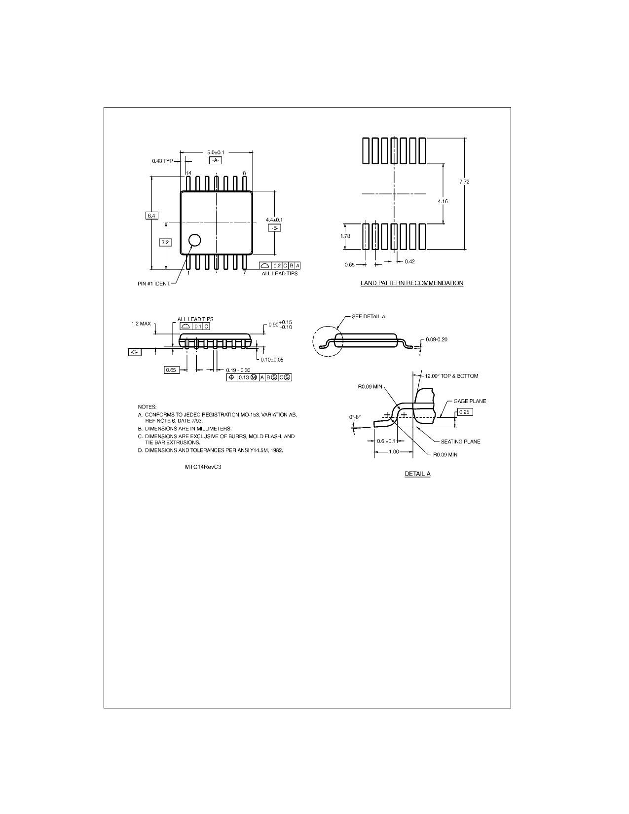
Physical Dimensions inches (millimeters) unless otherwise noted (Continued)
14-Lead Thin Shrink Small Outline Package (TSSOP), JEDEC MO-153, 4.4mm Wide
Package Number MTC14
Fairchild does not assume any responsibility for use of any circuitry described, no circuit patent licenses are implied and
Fairchild reserves the right at any time without notice to change said circuitry and specifications.
LIFE SUPPORT POLICY
FAIRCHILD’S PRODUCTS ARE NOT AUTHORIZED FOR USE AS CRITICAL COMPONENTS IN LIFE SUPPORT
DEVICES OR SYSTEMS WITHOUT THE EXPRESS WRITTEN APPROVAL OF THE PRESIDENT OF FAIRCHILD
SEMICONDUCTOR CORPORATION. As used herein:
1. Life support devices or systems are devices or systems
which, (a) are intended for surgical implant into the
body, or (b) support or sustain life, and (c) whose failure
to perform when properly used in accordance with
instructions for use provided in the labeling, can be rea-
sonably expected to result in a significant injury to the
user.
2. A critical component in any component of a life support
device or system whose failure to perform can be rea-
sonably expected to cause the failure of the life support
device or system, or to affect its safety or effectiveness.
www.fairchildsemi.com
5 www.fairchildsemi.com
5 Page | ||
| Páginas | Total 5 Páginas | |
| PDF Descargar | [ Datasheet 74ALVC32M.PDF ] | |
Hoja de datos destacado
| Número de pieza | Descripción | Fabricantes |
| 74ALVC32 | Low Voltage Quad 2-Input OR Gate with 3.6V Tolerant Inputs and Outputs | Fairchild Semiconductor |
| 74ALVC32 | Quad 2-input OR gate | NXP Semiconductors |
| 74ALVC32BQ | Quad 2-input OR gate | NXP Semiconductors |
| 74ALVC32D | Quad 2-input OR gate | NXP Semiconductors |
| Número de pieza | Descripción | Fabricantes |
| SLA6805M | High Voltage 3 phase Motor Driver IC. |
Sanken |
| SDC1742 | 12- and 14-Bit Hybrid Synchro / Resolver-to-Digital Converters. |
Analog Devices |
|
DataSheet.es es una pagina web que funciona como un repositorio de manuales o hoja de datos de muchos de los productos más populares, |
| DataSheet.es | 2020 | Privacy Policy | Contacto | Buscar |
