|
|
|
PDF 74LVC2G02 Data sheet ( Hoja de datos )
| Número de pieza | 74LVC2G02 | |
| Descripción | DUAL 2-INPUT NOR GATE | |
| Fabricantes | Diodes | |
| Logotipo | ||
Hay una vista previa y un enlace de descarga de 74LVC2G02 (archivo pdf) en la parte inferior de esta página. Total 11 Páginas | ||
|
No Preview Available !
74LVC2G02
DUAL 2-INPUT NOR GATE
Description
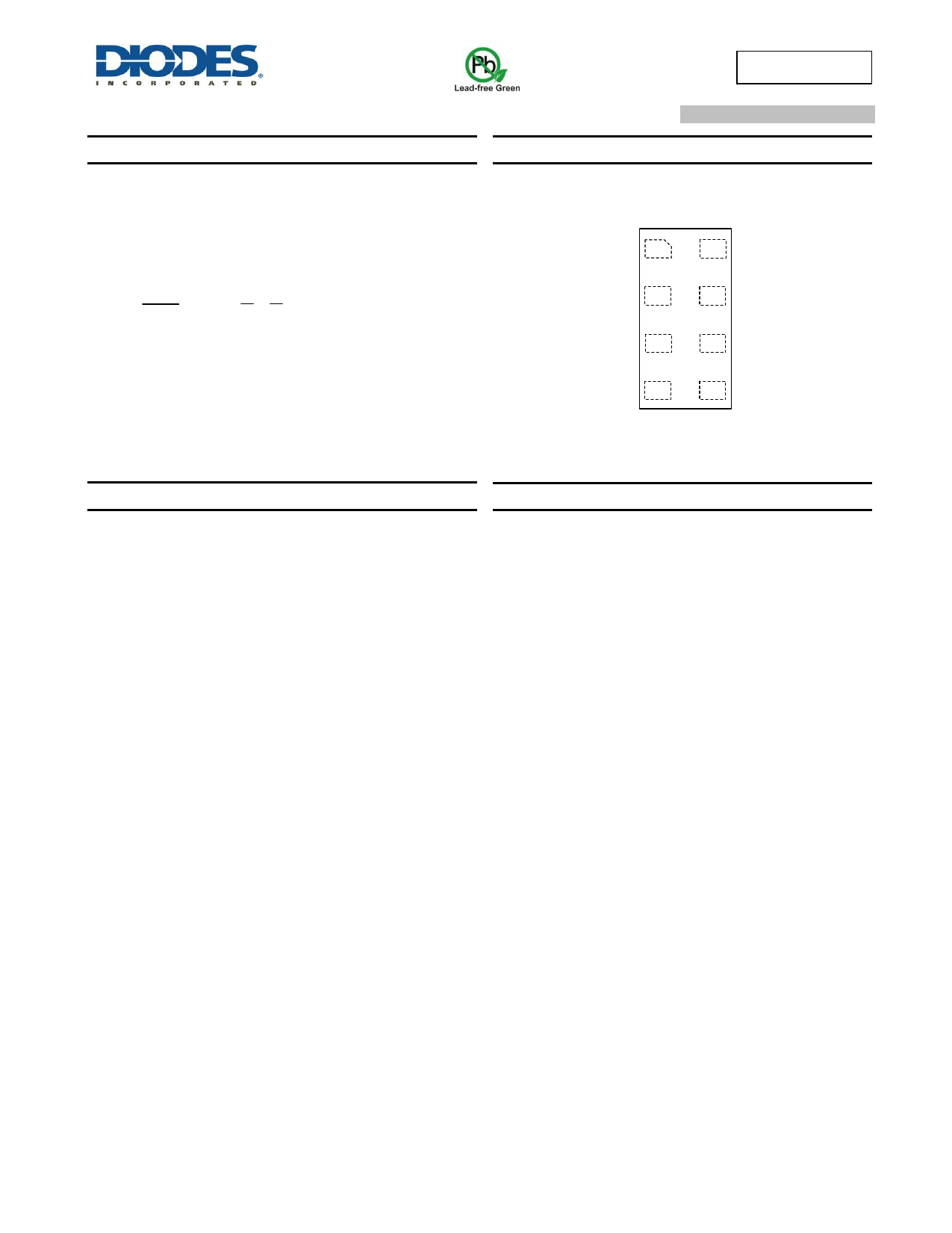
Pin Assignments
The 74LVC2G02 is a dual, two input NOR gate. Both gates have
push-pull outputs designed for operation over a power supply range
of 1.65V to 5.5V. The device is fully specified for partial power down
applications using IOFF. The IOFF circuitry disables the output,
preventing damaging current backflow when the device is powered
down. Each gate performs the positive Boolean function:
Y A B or Y A B
(Top View)
1A 1
8 VCC
1B 2
7 1Y
2Y 3
6 2B
GND 4
5 2A
Features
Wide Supply Voltage Range from 1.65 to 5.5V
± 24mA Output Drive at 3.3V
CMOS Low Power Consumption
IOFF Supports Partial-Power-Down Mode Operation
Inputs accept up to 5.5V
Schmitt Trigger Action at all inputs makes the circuit tolerant
for slower input rise and fall times. The hysteresis is typically
100mV at VCC = 3.0V.
ESD Protection Exceeds JESD 22
2000-V Human Body Model (A114)
Exceeds 1000-V Charged Device Model (C101)
Latch-Up Exceeds 100mA per JESD 78, Class I
Totally Lead-Free & Fully RoHS Compliant (Notes 1 & 2)
Halogen and Antimony Free. “Green” Device (Note 3)
X2-DFN2010-8
X2-DFN1410-8
X2-DFN1210-8
Applications
Voltage Level Shifting
General Purpose Logic
Power Down Signal Isolation
Wide Array of Products Such as:
PCs, Networking, Notebooks, Netbooks, PDAs
Tablet Computers, E-readers
Computer Peripherals, Hard Drives, CD/DVD ROMs
TVs, DVDs, DVRs, Set Top Boxes
Cell Phones, Personal Navigation / GPS
MP3 Players, Cameras, Video Recorders
Notes:
1. No purposely added lead. Fully EU Directive 2002/95/EC (RoHS) & 2011/65/EU (RoHS 2) compliant.
2. See http://www.diodes.com/quality/lead_free.html for more information about Diodes Incorporated’s definitions of Halogen- and
Antimony-free, "Green" and Lead-free.
3. Halogen- and Antimony-free "Green” products are defined as those which contain <900ppm bromine, <900ppm chlorine (<1500ppm total
Br + Cl) and <1000ppm antimony compounds.
74LVC2G02
Document number: DS37927 Rev 1 - 2
1 of 11
www.diodes.com
June 2016
© Diodes Incorporated
1 page 
Operating Characteristics
Parameter
Power Dissipation
Cpd Capacitance
Test
Conditions
f = 10MHz
VCC = 1.8V
Typ.
18
VCC = 2.5V
Typ.
18
VCC = 3.3V
Typ.
19
74LVC2G02
VCC = 5V
Typ.
22
Unit
pF
Package Characteristics
Symbol
Parameter
θJA
Thermal Resistance Junction-
to-Ambient
θJC
Thermal Resistance Junction-
to-Case
Package
X2-DFN2010-8
X2-DFN1410-8
X2-DFN1210-8
X2-DFN2010-8
X2-DFN1410-8
X2-DFN1210-8
Test Conditions
(Note 10)
(Note 10)
Min
—
—
—
—
—
—
Typ.
313
321
395
145
166
236
Max
—
—
—
—
—
—
Note: 10. Test condition for each package type: Device mounted on FR-4 substrate PC board, 2oz copper, with minimum recommended pad layout.
Unit
°C/W
°C/W
Switching Characteristics
Typical Values at TA = +25°C and nominal voltages 1.8V, 2.5V, 2.7V, 3.3V, and 5.0V. See Figure 1.
Parameter
From
Input
To
Output
VCC
TA = -40°C to +85°C
Min Typ Max
1.8V ± 0.15V
1.2
3.8
8.9
2.5V ± 0.2V
0.8
2.4
5.4
tpd
A or B
Y
2.7V
0.8 3.2 6.0
3.3V ± 0.3V
0.6
2.4
4.9
5.0V ± 0.5V
0.6
1.8
4.3
TA = -40°C to +125°C
Min Max
1.2 11.2
0.8 6.8
0.8 7.5
0.6 6.2
0.6 5.5
Unit
ns
74LVC2G02
Document number: DS37927 Rev 1 - 2
5 of 11
www.diodes.com
June 2016
© Diodes Incorporated
5 Page 
74LVC2G02
IMPORTANT NOTICE
DIODES INCORPORATED MAKES NO WARRANTY OF ANY KIND, EXPRESS OR IMPLIED, WITH REGARDS TO THIS DOCUMENT,
INCLUDING, BUT NOT LIMITED TO, THE IMPLIED WARRANTIES OF MERCHANTABILITY AND FITNESS FOR A PARTICULAR
PURPOSE (AND THEIR EQUIVALENTS UNDER THE LAWS OF ANY JURISDICTION).
Diodes Incorporated and its subsidiaries reserve the right to make modifications, enhancements, improvements, corrections or other changes
without further notice to this document and any product described herein. Diodes Incorporated does not assume any liability arising out of the
application or use of this document or any product described herein; neither does Diodes Incorporated convey any license under its patent or
trademark rights, nor the rights of others. Any Customer or user of this document or products described herein in such applications shall
assume all risks of such use and will agree to hold Diodes Incorporated and all the companies whose products are represented on Diodes
Incorporated website, harmless against all damages.
Diodes Incorporated does not warrant or accept any liability whatsoever in respect of any products purchased through unauthorized sales
channel.
Should Customers purchase or use Diodes Incorporated products for any unintended or unauthorized application, Customers shall indemnify
and hold Diodes Incorporated and its representatives harmless against all claims, damages, expenses, and attorney fees arising out of,
directly or indirectly, any claim of personal injury or death associated with such unintended or unauthorized application.
Products described herein may be covered by one or more United States, international or foreign patents pending. Product names and
markings noted herein may also be covered by one or more United States, international or foreign trademarks.
This document is written in English but may be translated into multiple languages for reference. Only the English version of this document is
the final and determinative format released by Diodes Incorporated.
LIFE SUPPORT
Diodes Incorporated products are specifically not authorized for use as critical components in life support devices or systems without the
express written approval of the Chief Executive Officer of Diodes Incorporated. As used herein:
A. Life support devices or systems are devices or systems which:
1. are intended to implant into the body, or
2. support or sustain life and whose failure to perform when properly used in accordance with instructions for
use provided in the labeling can be reasonably expected to result in significant injury to the user.
B. A critical component is any component in a life support device or system whose failure to perform can be reasonably
expected to cause the failure of the life support device or to affect its safety or effectiveness.
Customers represent that they have all necessary expertise in the safety and regulatory ramifications of their life support devices or systems,
and acknowledge and agree that they are solely responsible for all legal, regulatory and safety-related requirements concerning their products
and any use of Diodes Incorporated products in such safety-critical, life support devices or systems, notwithstanding any devices- or systems-
related information or support that may be provided by Diodes Incorporated. Further, Customers must fully indemnify Diodes Incorporated and
its representatives against any damages arising out of the use of Diodes Incorporated products in such safety-critical, life support devices or
systems.
Copyright © 2016, Diodes Incorporated
www.diodes.com
74LVC2G02
Document number: DS37927 Rev 1 - 2
11 of 11
www.diodes.com
June 2016
© Diodes Incorporated
11 Page | ||
| Páginas | Total 11 Páginas | |
| PDF Descargar | [ Datasheet 74LVC2G02.PDF ] | |
Hoja de datos destacado
| Número de pieza | Descripción | Fabricantes |
| 74LVC2G00 | Dual 2-input NAND gate | Panasonic Semiconductor |
| 74LVC2G00 | DUAL 2-INPUT NAND GATE | Diodes |
| 74LVC2G00 | Dual 2-input NAND gate | NXP Semiconductors |
| 74LVC2G00-Q100 | Dual 2-input NAND gate | NXP Semiconductors |
| Número de pieza | Descripción | Fabricantes |
| SLA6805M | High Voltage 3 phase Motor Driver IC. |
Sanken |
| SDC1742 | 12- and 14-Bit Hybrid Synchro / Resolver-to-Digital Converters. |
Analog Devices |
|
DataSheet.es es una pagina web que funciona como un repositorio de manuales o hoja de datos de muchos de los productos más populares, |
| DataSheet.es | 2020 | Privacy Policy | Contacto | Buscar |