74ABT5074N 반도체 회로 부품 판매점
Synchronizing dual D-type flip-flop with metastable immune characteristics
|
|
|
NXP Semiconductors |
Philips Semiconductors Advanced BiCMOS Products
Synchronizing dual D-type flip-flop
with metastable immune characteristics
Product specification
74ABT5074
FEATURES
• Metastable immune characteristics
• Pin compatible with 74F74 and 74F5074
• Typical fMAX = 200MHz
• Output skew guaranteed less than 2.0ns
• High source current (IOH = 15mA) ideal for clock driver
applications
• Output capability: +20mA/–15mA
• Latch-up protection exceeds 500mA per Jedec JC40.2 Std 17
• ESD protection exceeds 2000V per MIL STD 883 Method 3015
and 200V per Machine Model
DESCRIPTION
The 74ABT5074 is a dual positive edge-triggered D-type flip-flop
featuring individual data, clock, set and reset inputs; also true and
complementary outputs.
Set (SDn) and reset (RDn) are asynchronous active low inputs and
operate independently of the clock (CPn) input. Data must be stable
just one setup time prior to the low-to-high transition of the clock for
guaranteed propagation delays.
Clock triggering occurs at a voltage level and is not directly related
to the transition time of the positive-going pulse. Following the hold
time interval, data at the Dn input may be changed without affecting
the levels of the output.
The 74ABT5074 is designed so that the outputs can never display a
metastable state due to setup and hold time violations. If setup time
and hold time are violated the propagation delays may be extended
beyond the specifications but the outputs will not glitch or display a
metastable state. Typical metastability parameters for the
74ABT5074 are:
τ ≅ 94ps and To ≅ 1.3 × 10⁷ sec
where τ represents a function of the rate at which a latch in a
metastable state resolves that condition and T0 represents a
function of the measurement of the propensity of a latch to enter a
metastable state.
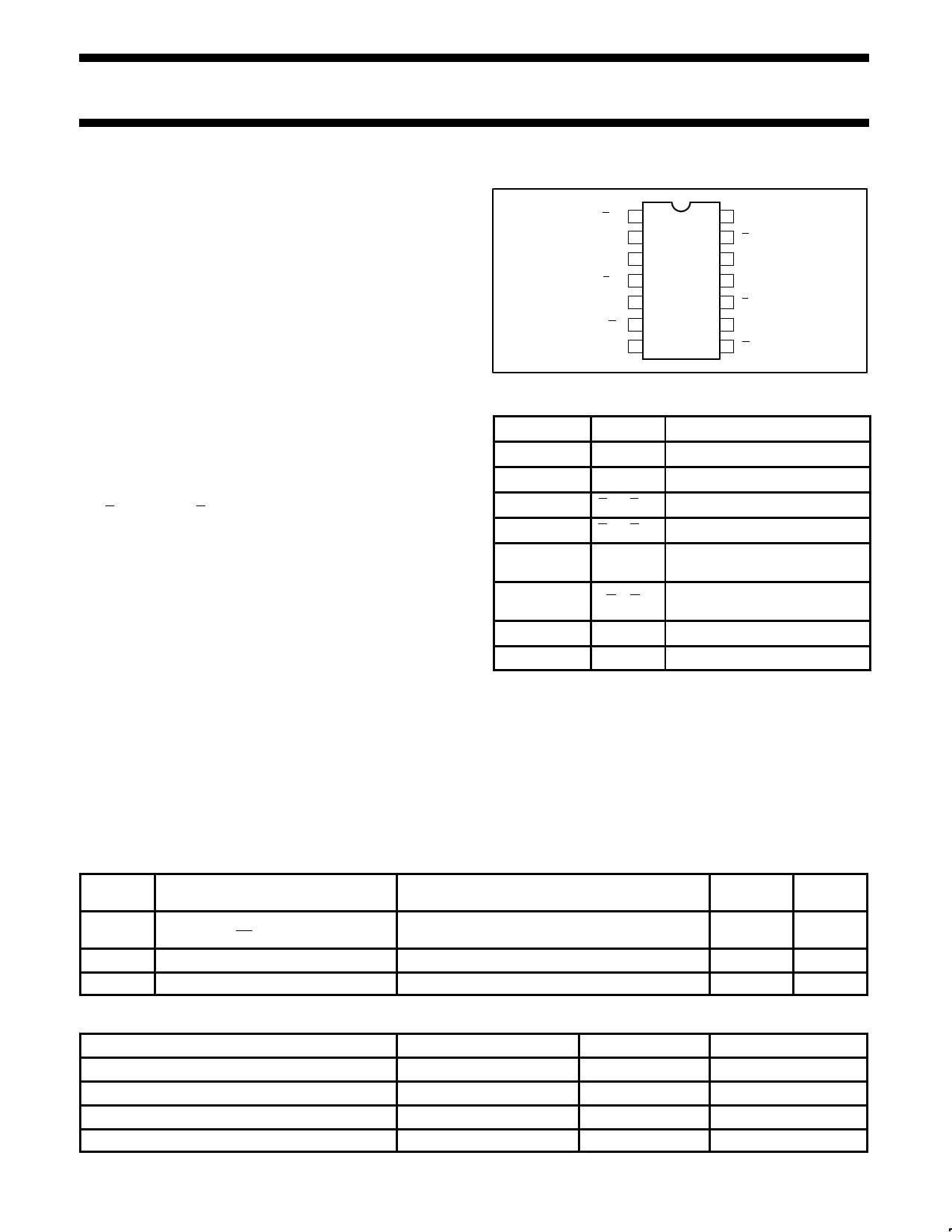
PIN CONFIGURATION
RD0 1
D0 2
CP0 3
SD0 4
Q0 5
Q0 6
GND 7
14 VCC
13 RD1
12 D1
11 CP1
10 SD1
9 Q1
8 Q1
SA00001
PIN DESCRIPTION
PIN NUMBER SYMBOL
NAME AND FUNCTION
2, 12
D0, D1 Data inputs
3, 11
CP0, CP1 Clock inputs (active rising edge)
4, 10
SD0, SD1 Set inputs (active-Low)
1, 13
RD0, RD1 Reset inputs (active-Low)
5, 9
Q0, Q1
Data outputs (active-Low),
non-inverting
6, 8
Q0, Q1
Data outputs (active-Low),
inverting
7 GND Ground (0V)
14 VCC Positive supply voltage
QUICK REFERENCE DATA
SYMBOL
PARAMETER
tPLH Propagation delay
tPHL CPn to Qn or Qn
CIN Input capacitance
ICC Total supply current
CONDITIONS
Tamb = 25°C; GND = 0V
CL = 50pF; VCC = 5V
VI = 0V or VCC
Outputs disabled; VCC =5.5V
TYPICAL
2.8
2.4
3
2
UNIT
ns
pF
µA
ORDERING INFORMATION
PACKAGES
14-pin plastic DIP
14-pin plastic SOL
14-pin plastic shrink small outline SSOP Type II
14-pin plastic thin shrink small outline (TSSOP) Type I
TEMPERATURE RANGE
–40°C to +85°C
–40°C to +85°C
–40°C to +85°C
–40°C to +85°C
ORDER CODE
74ABT5074N
74ABT5074D
74ABT5074DB
74ABT5074PW
DRAWING NUMBER
SOT27-1
SOT108-1
SOT337-1
SOT402-1
December 15, 1994
1
853-1775 14470

Philips Semiconductors Advanced BiCMOS Products
Synchronizing dual D-type flip-flop
with metastable immune characteristics
Product specification
74ABT5074
LOGIC SYMBOL
2 12
D0 D1
3 CP0
4 SD0
1 RD0
11 CP1
10 SD1
13 RD1
Q0 Q0 Q1 Q1
VCC = Pin 14
GND = Pin 7
56 98
LOGIC DIAGRAM
SD 4, 10
RD 1, 13
CP 3, 11
D 2, 12
VCC = Pin 14
GND = Pin 7
IEC/IEEE SYMBOL
SA00002
4
S
3
C1
2
1D
1
R
10
S
11
C2
12
2D
13
R
5
6
9
8
SA00003
5, 9
Q
6, 8
Q
SF00048
FUNCTION TABLE
INPUTS
SD RD CP
D
OUTPUTS
QQ
OPERATING
MODE
LHXX
H
L Asynchronous set
HLXX
L
H Asynchronous reset
L LXX
L
H Undetermined*
HH↑ h
H
L Load ”1”
HH↑
l
L
H Load ”0”
H H ↑ X NC NC Hold
NOTES:
H = High voltage level
h = High voltage level one setup time prior to low-to-high clock
transition
L = Low voltage level
l = Low voltage level one setup time prior to low-to-high clock
transition
NC= No change from the previous setup
X = Don’t care
↑ = Low-to-high clock transition
↑ = Not low-to-high clock transition
* = This setup is unstable and will change when either set or
reset return to the high level
December 15, 1994
2
|
PDF 파일 내의 페이지 : 총 7 페이지
제조업체: NXP Semiconductors
( nxp )
74ABT5074N flip-flop
데이터시트 다운로드 :
[ 74ABT5074N.PDF ]
[ 74ABT5074N 다른 제조사 검색 ]
국내 전력반도체 판매점
상호 : 아이지 인터내셔날
전화번호 : 051-319-2877
[ 홈페이지 ]
IGBT, TR 모듈, SCR, 다이오드모듈, 각종 전력 휴즈
( IYXS, Powerex, Toshiba, Fuji, Bussmann, Eaton )
전력반도체 문의 : 010-3582-2743
관련 데이터시트
74ABT5074
Synchronizing dual D-type flip-flop with metastable immune characteristics - NXP Semiconductors

74ABT5074D
Synchronizing dual D-type flip-flop with metastable immune characteristics - NXP Semiconductors
74ABT5074DB
Synchronizing dual D-type flip-flop with metastable immune characteristics - NXP Semiconductors
74ABT5074N
Synchronizing dual D-type flip-flop with metastable immune characteristics - NXP Semiconductors
74ABT5074PW
Synchronizing dual D-type flip-flop with metastable immune characteristics - NXP Semiconductors