|
|
|
PDF IX2120 Data sheet ( Hoja de datos )
| Número de pieza | IX2120 | |
| Descripción | 1200V High and Low Side Gate Driver | |
| Fabricantes | IXYS | |
| Logotipo | ||
Hay una vista previa y un enlace de descarga de IX2120 (archivo pdf) en la parte inferior de esta página. Total 13 Páginas | ||
|
No Preview Available !
INTEGRATED CIRCUITS DIVISION
Driver Characteristics
Parameter
VOFFSET
IO +/- (Source/Sink)
VOUT
ton/toff
Rating
1200
2/2
15-20
250/210
Units
V
A
V
ns
Features
• Floating Channel for Bootstrap Operation to +1200V
• Outputs Capable of Sourcing and Sinking 2A
• Gate Drive Supply Range From 15V to 20V
• Enhanced Robustness due to SOI Process
• Tolerant to Negative Voltage Transients:
dV/dt Immune
• 3.3V Logic Compatible
• Undervoltage Lockout for Both High-Side and
Low-Side Outputs
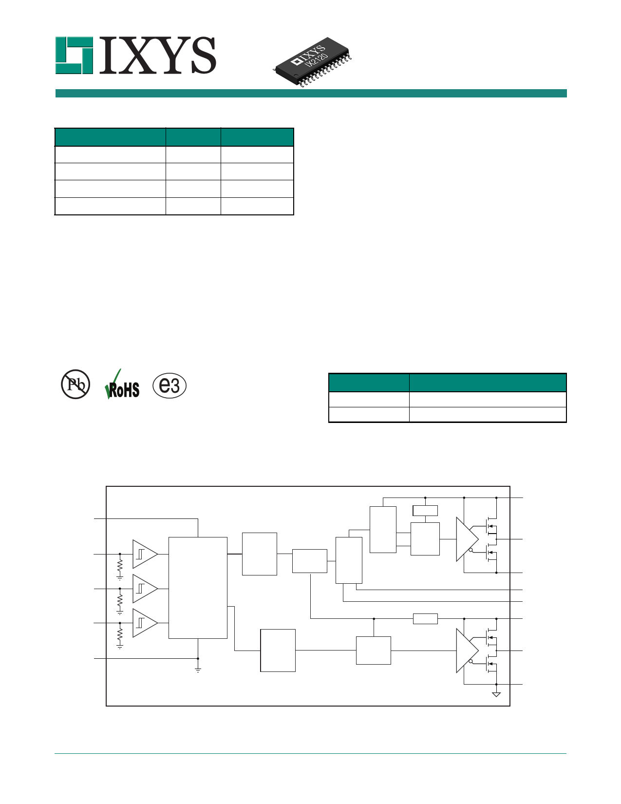
IX2120 Functional Block Diagram
IX2120
1200V High and Low Side
Gate Driver
Description
The IX2120 is a high voltage integrated circuit that can
drive high speed MOSFETs and IGBTs that operate at
up to +1200V. The IX2120 is configured with
independent high-side and low-side referenced output
channels, both of which can source and sink 2A. The
floating high-side channel can drive an N-channel
power MOSFET or IGBT 1200V from the common
reference.
Manufactured on IXYS Integrated Circuits Division's
proprietary high-voltage BCDMOS on SOI (silicon on
insulator) process, the IX2120 is extremely robust, and
is virtually immune to negative transients. The UVLO
circuit prevents turn-on of the MOSFET or IGBT until
there is sufficient VBS or VCC supply voltage.
The IX2120 is available in a 28-pin SOIC package.
Ordering Information
Part
IX2120B
IX2120BTR
Description
28-Pin SOIC (28/Tube)
28-Pin SOIC (1000/Reel)
VB
VDD
High
Voltage
UVLO
Level R C
Level
Shift
Shift
Mid
Q
S
Buffer
HO
HIN
Input Control Logic
VDD / VCC
VSS / COM
Pulse
Generator
Voltage
Level
Shift
&
VS
SD Cycle-by-Cycle
Edge-Triggered
Shutdown
VBM
VSM
LIN
UVLO
VCC
Level
VSS
Shift
VDD / VCC
VSS / COM
LS Delay
Control
Buffer
LO
COM
DS-IX2120-R02
www.ixysic.com
1
1 page 
INTEGRATED CIRCUITS DIVISION
IX2120
1.6 Dynamic Electrical Characteristics
VCC, VDD=15V; VBS, VBMSM=13.5V; CL=1000 pF; and VSS=COM unless otherwise specified. See “Test
Waveforms” on page 6.
Parameter
Turn-On propagation Delay
Turn-Off propagation Delay
Shutdown propagation Delay
Turn-On Rise Time
Turn-Off Fall Time
Delay Matching, HS & LS Turn-On/Off
Conditions
VS=0V
VSM=600V
VS=1200V
-
-
-
Symbol Min Typ Max Units
ton - 254 -
toff - 213 -
tSD - 207 - ns
tr - 9.4 -
tf - 9.7 -
MT -
- 60
1.7 Static Electrical Characteristics
VCC, VBMSM, VBS, VDD=15V, and VSS=COM unless otherwise specified. The VIN, VTH, and IIN parameters are
referenced to VSS and are applicable to all three logic input leads: HIN, LIN, and SD. The VO and IO parameters are
referenced to COM and are applicable to the respective output leads: HO or LO.
Parameter
Conditions
Symbol Min Typ Max Units
Logic “1” Input Voltage
Logic “0” Input Voltage
Logic “1” Input Voltage
Logic “0” Input Voltage
High-Level Output Voltage, VBIAS-VO
Low-Level Output Voltage, VO
High Offset Supply Leakage Current
Middle Offset Supply Leakage Current
Quiescent VBS Supply Current
Quiescent VBMSM Supply Current
Quiescent VCC Supply Current
Quiescent VDD Supply Current
Logic “1” Input Bias Current
Logic “0” Input Bias Current
VBS Supply Undervoltage Positive Going Threshold
VBS Supply Undervoltage Negative Going Threshold
VCC Supply Undervoltage Positive Going Threshold
VCC Supply Undervoltage Negative Going Threshold
Output High Short Circuit Pulsed Current
Output Low Short Circuit Pulsed Current
VDD=15V
VDD=3V
IO=0A
IO=20mA
VB=VS=600V
VBM=VSM=600V
VIN=0V or VDD
VIN=0V or VDD
VIN=0V or VDD
VIN=0V or VDD
VIN=VDD
VIN=0V
-
-
-
-
VO=0V, VIN=VDD , PW10s
VO=15V, VIN=0V, PW10s
VIH
VIL
VIH
VIL
VOH
VOL
IHLK
IMLK
IQBS
IQBMSM
IQCC
IQDD
IIN+
IIN-
VBSUV+
VBSUV-
VCCUV+
VCCUV-
IO+
IO-
9.5
-
2.5
-
-
-
-
-
-
-
-
-
-
-
7.5
7
7.4
7
2
2
- -V
-6
- -V
- 0.8
1.6 2.5
V
- 0.15
32 60
32 60
187 310
A
487 730
300 420
-1
22 40
A
-5
8.4 9.7
7.8 9.4
V
8.4 9.6
7.8 9.4
--
A
--
R02 www.ixysic.com
5
5 Page 
INTEGRATED CIRCUITS DIVISION
IX2120
High Level Output Voltage
vs. Supply Voltage
5
4
3
2
1
0
10 12 14 16 18 20
Supply Voltage (V)
200
160
120
80
40
0
10
Low Level Output Voltage
vs. Supply Voltage
12 14 16 18
VCC Supply Voltage (V)
20
R02 www.ixysic.com
11
11 Page | ||
| Páginas | Total 13 Páginas | |
| PDF Descargar | [ Datasheet IX2120.PDF ] | |
Hoja de datos destacado
| Número de pieza | Descripción | Fabricantes |
| IX2120 | 1200V High and Low Side Gate Driver | IXYS |
| IX2127 | High-Voltage Power MOSFET & IGBT Driver | Clare |
| IX2127 | High-Voltage Power MOSFET & IGBT Driver | IXYS |
| Número de pieza | Descripción | Fabricantes |
| SLA6805M | High Voltage 3 phase Motor Driver IC. |
Sanken |
| SDC1742 | 12- and 14-Bit Hybrid Synchro / Resolver-to-Digital Converters. |
Analog Devices |
|
DataSheet.es es una pagina web que funciona como un repositorio de manuales o hoja de datos de muchos de los productos más populares, |
| DataSheet.es | 2020 | Privacy Policy | Contacto | Buscar |