|
|
|
PDF BL0202B Data sheet ( Hoja de datos )
| Número de pieza | BL0202B | |
| Descripción | High Efficiency | |
| Fabricantes | Sanken | |
| Logotipo | ||
Hay una vista previa y un enlace de descarga de BL0202B (archivo pdf) en la parte inferior de esta página. Total 26 Páginas | ||
|
No Preview Available !
High Efficiency
For LED Backlight 2ch LED Driver IC
BL0200 Series
General Descriptions
BL0200 series are 2ch output LED driver IC for LED
backlight, and it can do dimming to 0.02 % by external
PWM signal.
This IC realizes a high efficiency by the boost
convertor control that absorbs variability on VF.
The product easily achieves high cost-performance
LED drive system with few external components and
enhanced protection functions.
Package
SOP18
Features and Benefit
Boost convertor
● Current-Mode type PWM Control
● PWM frequency is 100 kHz o r 200 kHz
● Maximum On Duty is 90 %
LED current control
● Individual PWM Dimming Control
● Analog Dimming
● High contrast ratio is 1 / 5000
● Accuracy of Reg output voltage is ± 1.5 % or ± 2 %
Protection functions
● Enable Function of IC (BL0202B, BL0202C)
● Error Signal Output (BL0200C)
● Overcurrent Protection for Boost Circuit (OCP)
----------------------------------------------Pulse-by-pulse
● Overcurrent Protection for LED Output (LED_OCP)
----------------------------------------------Pulse-by-pulse
● Overvoltage Protection (OVP) ----------- Auto restart
● Output Open/Short Protection ------------ Auto restart
● Thermal Shutdown (TSD)----------------- Auto restart
Not to scale
Lineup
Products
BL0202C
BL0202B
BL0200C
Frequency
200 kHz
100 kHz
VREG
Accuracy
± 1.5 %
Built-in Function
Enable Function of
IC
200 kHz ± 2 % Error Signal Output
Applications
● LED backlights
● LED lighting etc.
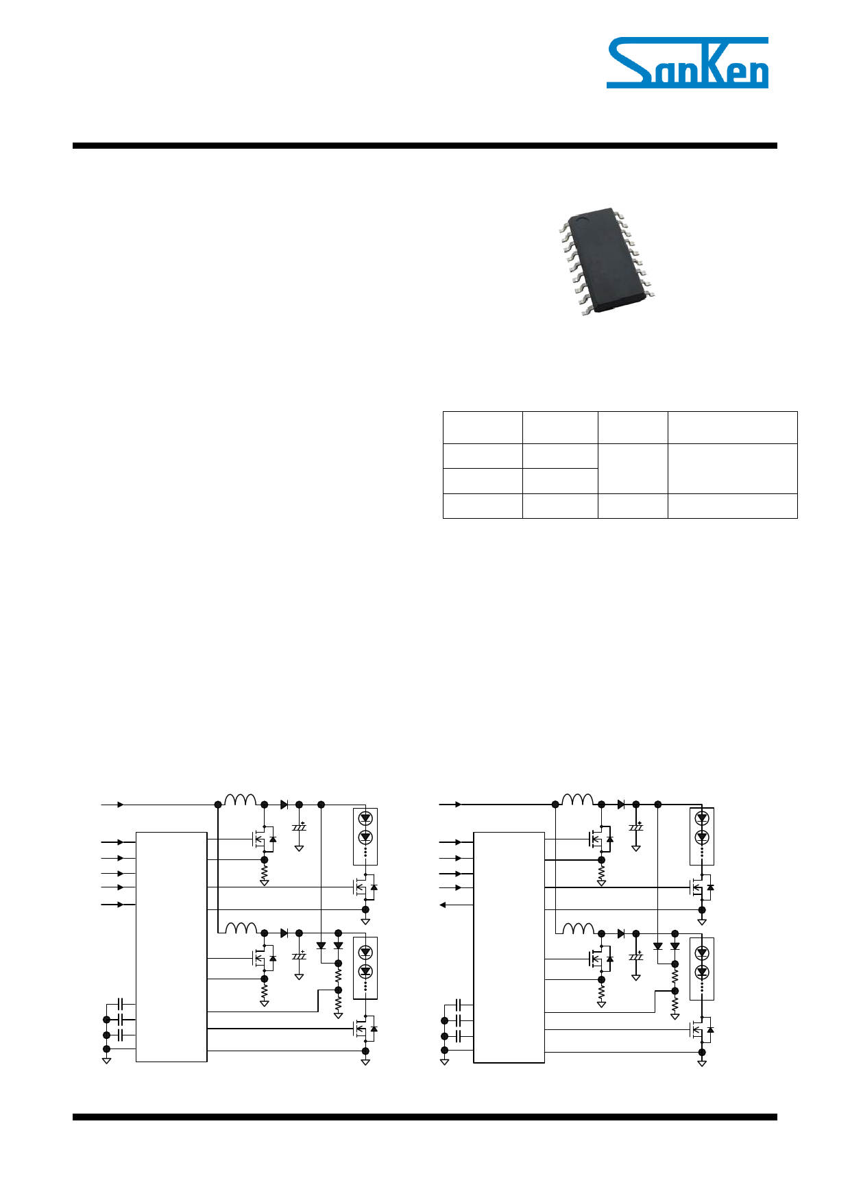
Typical Application Circuit
BL0202B/C
VCC
DRV1
VREF
PWM1
PWM2
OC1
SW1
EN IFB1
DRV2
OC2
REG
COMP1
COMP2
GND
OVP
SW2
IFB2
TC_BL0202_1_R1
BL0200C
VCC
DRV1
VREF
PWM1
PWM2
OC1
SW1
ER IFB1
DRV2
OC2
REG
COMP1
COMP2
GND
OVP
SW2
IFB2
TC_BL0200C_1_R1
BL0200-DS Rev.2.3
May. 15, 2014
SANKEN ELECTRIC CO.,LTD.
1
1 page 
BL0200 Series
Parameter
COMP Pin Minimum Output
Voltage
Transconductance
COMP Pin Source Current
COMP Pin Sink Current
COMP Pin Charge Current at
Startup
COMP Pin Reset Current
EN Pin
Symbol
VCOMP1(MIN)
VCOMP2(MIN)
gm
ICOMP1(SRC)
ICOMP2(SRC)
ICOMP1(SNK)
ICOMP2(SNK)
ICOMP1(S)
ICOMP2(S)
ICOMP1(R)
ICOMP2(R)
Test
Conditions
VIFB1 = 2.0 V
VIFB2 = 2.0 V
VIFB1 = 0.7 V
VIFB2 = 0.7 V
VIFB1 = 1.5 V
VIFB2 = 1.5 V
VCOMP1 = 0 V
VCOMP2 = 0 V
Pins
4–9
15 – 9
−
4–9
15 – 9
4–9
15 – 9
4–9
15 – 9
4–9
15 – 9
Operation Start EN Pin Voltage
Operation Stop EN Pin Voltage
EN Pin Sink Current
VEN(ON)
VEN(OFF)
IEN
VEN = 3 V
17 – 9
17 – 9
17 – 9
ER Pin
ER Pin Sink Current during
Non-Alarm
IER
VER = 1 V
17 – 9
Boost Parts Overcurrent Protection (OCP)
OC Pin Overcurrent Protection
Threshold Voltage
VOCP1
VOCP2
VCOMP1
= VCOMP2
= 4.5 V
6–9
13 – 9
Overvoltage Protection (OVP)
OVP Pin Overvoltage
Protection Threshold Voltage
OVP Pin OVP Release
Threshold Voltage
VOVP
VOVP(OFF)
2–9
2–9
PWM Pin
PWM Pin ON Threshold
Voltage
PWM Pin OFF Threshold
Voltage
PWM Pin Impedance
VPWM1(ON)
VPWM2(ON)
VPWM1(OFF)
VPWM2(OFF)
RPWM1
RPWM2
SW / DRV Pin
SW Pin Source Current
SW Pin Sink Current
DRV Pin Source Current
DRV Pin Sink Current
ISW1(SRC)
ISW2(SRC)
ISW1(SNK)
ISW2(SNK)
IDRV1(SRC)
IDRV2(SRC)
IDRV1(SNK)
IDRV2(SNK)
Thermal Shutdown Protection (TSD)
3–9
16 – 9
3–9
16 – 9
3–9
16 – 9
8–9
11 – 9
8–9
11 – 9
7–9
12 – 9
7–9
12 – 9
Thermal Shutdown Activating
Temperature
Hysteresis Temperature of TSD
Tj(TSD)
Tj(TSD)HYS
−
−
Thermal Resistance
Thermal Resistance from
Junction to Ambient
θj-A
−
Min. Typ. Max. Unit
− 0 0.2
− 640 −
−77 −57 −37
V
µS
µA
37 57
−19 −11
77
−3
µA
µA
200 360 520 µA
1.2 2.0 2.6 V
0.8 1.4 1.8 V
20 55 120 µA
2.5 4.4 6.3 mA
0.57 0.60 0.63 V
2.85 3.00 3.15
2.60 2.75 2.90
V
V
1.4 1.5 1.6
0.9 1.0 1.1
100 200 300
V
V
kΩ
− −85 −
− 220 −
− −0.36 −
− 0.85 −
mA
mA
A
A
125 − − °C
− 65 − °C
− − 95 °C/W
Notes
BL0202B
BL0202C
BL0200C
BL0200-DS Rev.2.3
May. 15, 2014
SANKEN ELECTRIC CO.,LTD.
5
5 Page 
BL0200 Series
increase of the COMP pin voltage, and the output power
increases (Soft start operation). Thus, power stresses on
components are reduced.
When the VCC pin voltage decreases to the operation
stop voltage or less, or the Auto Restart operation (see
the Section 8.7 Protection Function) after protection is
achieved, then the control circuit stops switching
operation, and capacitors at the COMP pin are
discharged by the COMP Pin Reset Current,
ICOMP(R) = 360 µA simultaneously. The soft start
operation is achieved at restart.
The IC is operated by Auto Restart 1 at startup
operation. See the Section 8.7 Protection Function about
the caution of startup operation.
VIFB(COMP.VR) is determined by the VREF pin voltage,
as shown in Figure 8-4. When VREF pin voltage is 1V,
the value of VIFB(COMP.VR) becomes 0.60 V.
VIFB(COMP.VR)
1.2V
0.6V
0.15V
0.25V 1V
2V
VREF pin voltage
Figure 8-4 VREF pin voltage versus IFB pin voltage at
COMP charge switching
VCC pin voltage decreases to the Operation Stop
Voltage, VCC(OFF) = 8.6 V, the control circuit stops
operation, by the UVLO (Undervoltage Lockout) circuit,
and reverts to the state before startup.
The value of R39 connected to EN pin is set as
follows;
R39 VEN_ IN VEN(ON) (max)
IEN (max)
VEN_ IN 2.6(V)
120(A)
(8-1)
Where,
VEN_IN is EN pin input voltage (less than absolute value
of EN pin voltage, 5 V ). VEN(ON)(max) is the maximum
rating of EN Pin Operation Start Voltage. IEN(max) is
the maximum rating of EN Pin Sink Current.
In case VEN_IN = 3.5V, the value of R39 should be set
7.5 kΩ or less.
External power supply
ON/OFF
R39
C8
C7 VEN_IN
8
VCC
BL0202B/C
5
EN
COMP1
4
C22
R42
C16
C15
PWM1 3
GND
9
8.2 Startup Operation(BL0202B, BL0202C)
BL0202B and BL0202C have Enable Function. Figure
8-5 shows the peripheral circuit of VCC pin and EN pin,
Figure 8-6 shows the operational waveforms.
The VCC pin is the power supply input for control
circuit from the external power supply. The EN pin is
ON/OFF signal input from the external circuit.
When the both VCC pin voltage, VCC, and EN pin
voltage, VEN, increase to the each operation voltage or
more, the control circuit starts operation (VCC ≥
VCC(ON) = 9.6 V and VEN ≥ VEN(ON) = 2.0 V).
After that, when the PWM pin voltage exceeds the
PWM Pin ON Threshold Voltage, VPWM(ON) of 1.5 V
(less than absolute maximum voltage of 5 V), the COMP
Pin Charge Current at Startup, ICOMP(S) = −11 µA, flows
from the COMP pin. This charge current flows to
capacitors at the COMP pin. When the COMP pin
voltage increases to the COMP Pin Voltage at Oscillation
Start, VCOMP(ON) = 0.50 V or more, the control circuit
starts switching operation.
As shown in Figure 8-2, when the EN pin voltage
decreases to the Operation Stop Voltage VEN(OFF) = 1.4 V
or less, the control circuit stops operation. And when the
Figure 8-5 The peripheral circuit of VCC pin and EN pin
VCC pin voltage
VCC(ON)
0
EN pin voltage
VEN(ON)
0
REG pin voltage
0
COMP pin voltage
VCOMP(ON)
VCOMP(OFF)
0
IC switching status
OFF
VCC(OFF)
VEN(OFF)
ON OFF
ON OFF
Figure 8-6 Operational waveforms
BL0200-DS Rev.2.3
May. 15, 2014
SANKEN ELECTRIC CO.,LTD.
11
11 Page | ||
| Páginas | Total 26 Páginas | |
| PDF Descargar | [ Datasheet BL0202B.PDF ] | |
Hoja de datos destacado
| Número de pieza | Descripción | Fabricantes |
| BL0202B | High Efficiency | Sanken |
| BL0202C | High Efficiency | Sanken |
| Número de pieza | Descripción | Fabricantes |
| SLA6805M | High Voltage 3 phase Motor Driver IC. |
Sanken |
| SDC1742 | 12- and 14-Bit Hybrid Synchro / Resolver-to-Digital Converters. |
Analog Devices |
|
DataSheet.es es una pagina web que funciona como un repositorio de manuales o hoja de datos de muchos de los productos más populares, |
| DataSheet.es | 2020 | Privacy Policy | Contacto | Buscar |