|
|
|
PDF DK2051 Data sheet ( Hoja de datos )
| Número de pieza | DK2051 | |
| Descripción | HIGH PERFORMANCE WIDEBAND RF PLL/VCO | |
| Fabricantes | RF Micro Devices | |
| Logotipo | ||
Hay una vista previa y un enlace de descarga de DK2051 (archivo pdf) en la parte inferior de esta página. Total 30 Páginas | ||
|
No Preview Available !
RF2051RF2051
HIGH PERFORMANCE WIDEBAND RF PLL/VCO WITH
INTEGRATED RF MIXERS
Package: QFN, 32-Pin, 5mmx5mm
Features
30MHz to 2.5GHz Frequency
Range
Fractional-N Synthesizer
Very Fine Frequency Resolution
1.5Hz for 26MHz Reference
Low Phase Noise VCO
On-Chip Crystal-Sustaining
Circuit With Programmable
Loading Capacitors
Two High-Linearity RF Mixers
Integrated LO Buffers
Mixer Input IP3 +18dBm
Mixer Bias Adjustable for Low
Power Operation
Full Duplex Mode
2.7V to 3.6V Power Supply
Low Current Consumption
55mA to 75mA at 3V
3-Wire Serial Interface
Applications
CATV Head-Ends
Digital TV Up/Down Converters
Digital TV Repeaters
Multi-Dwelling Units
Cellular Repeaters
Frequency Band Shifters
UHF/VHF Radios
Diversity Receivers
Software Defined Radios
Satellite Communications
Super-Heterodyne Radios
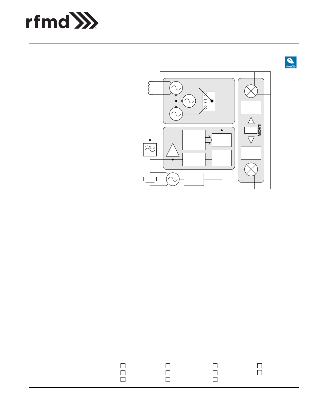
VCO
LO
divider
Synth
Frac-N
sequence
generator
Charge
pump
N divider
Phase /
freq
detector
Mux
LO
divider
Ref
divider
Functional Block Diagram
Product Description
The RF2051 is a low power, high performance, wideband RF frequency conversion
chip with integrated local oscillator (LO) generation and a pair of RF mixers. The RF
synthesizer includes an integrated fractional-N phase locked loop with voltage con-
trolled oscillators (VCOs) and dividers to produce a low-phase noise LO signal with a
very fine frequency resolution. The buffered LO output drives the built-in RF mixers
which convert the signal into the required frequency band. The mixer bias current
can be programmed dependent on the required performance and available supply
current. The LO generation blocks have been designed to continuously cover the
frequency range from 300MHz to 2400MHz. The RF mixers are very broad band
and operate from 30MHz to 2500MHz at the input and output, enabling both up
and down conversion. An external crystal of between 10MHz and 52MHz or an
external reference source of between 10MHz and 104MHz can be used with the
RF2051 to accommodate a variety of reference frequency options.
All on-chip registers are controlled through a simple three-wire serial interface. The
RF2051 is designed for 2.7V to 3.6V operation for compatibility with portable, bat-
tery powered devices. It is available in a plastic 32-pin, 5mmx5mm QFN package.
Optimum Technology Matching® Applied
GaAs HBT
GaAs MESFET
InGaP HBT
SiGe BiCMOS
Si BiCMOS
SiGe HBT
GaAs pHEMT
Si CMOS
Si BJT
GaN HEMT
RF MEMS
DS140110
RF MICRO DEVICES®, RFMD®, Optimum Technology Matching®, Enabling Wireless Connectivity™, PowerStar®, POLARIS™ TOTAL RADIO™ and UltimateBlue™ are trademarks of RFMD, LLC. BLUETOOTH is a trade-
mark owned by Bluetooth SIG, Inc., U.S.A. and licensed for use by RFMD. All other trade names, trademarks and registered trademarks are the property of their respective owners. ©2006, RF Micro Devices, Inc.
7628 Thorndike Road, Greensboro, NC 27409-9421 · For sales or technical
support, contact RFMD at (+1) 336-678-5570 or [email protected].
1 of 39
1 page 
RF2051
Parameter
Mixer 1/2, cont.
IIP3
Low Current Setting
High Linearity Setting
Pin1dB
Low Current Setting
High Linearity Setting
RF and IF Port Frequency Range
Mixer Input Return Loss
Voltage Controlled Oscillator
Open Loop Phase Noise at 1MHz
Offset
2GHz LO Frequency
1GHz LO Frequency
500MHz LO Frequency
Reference Oscillator
Xtal Frequency
External Reference Frequency
Reference Divider Ratio
External Reference Input Level
Local Oscillator
Synthesizer Output Frequency
Phase Detector Frequency
Closed Loop Phase-Noise at
10kHz Offset
2GHz LO Frequency
1GHz LO Frequency
500MHz LO Frequency
Specification
Min. Typ. Max.
+10
+18
+2
+12
30 2500
10
-130
-135
-140
10 52
10 104
17
500 800 1500
300 2400
52
-90
-95
-102
Unit Condition
dBm
dBm
dBm
dBm
MHz
dB 100 differential
dBc/Hz
dBc/Hz
dBc/Hz
MHz
MHz
mVP-P
AC-coupled
MHz
MHz
dBc/Hz
dBc/Hz
dBc/Hz
Dependant on VCO 3 external inductor. After
LO dividers.
26MHz phase detector frequency
DS140110
7628 Thorndike Road, Greensboro, NC 27409-9421 · For sales or technical
support, contact RFMD at (+1) 336-678-5570 or [email protected].
5 of 39
5 Page 
RF2051
Detailed Description
The RF2051 is a wideband RF frequency converter chip which includes a fractional-N phase-locked loop, a crystal oscillator cir-
cuit, a low noise VCO core, a LO signal multiplexer, two buffer circuits and two RF mixers. Synthesizer programming, device con-
figuration and control are achieved through a mixture of hardware and software controls. All on-chip registers are programmed
through a simple three-wire serial interface.
VCO
The VCO core in the RF2051 consists of three VCOs which, in conjunction with the integrated 2/4 LO divider, cover the LO
range from 300MHz to 2400MHz.
VCO Tank Inductor VCO Frequency Range DIV 2
1
Internal
1800MHz to 2400MHz
900MHz to 1200MHz
2
Internal
1500MHz to 2100MHz
750MHz to 1050MHz
3
External
1200MHz to 1600MHz*
600MHz to 800MHz
*The frequency of VCO3 is set by external inductors and can be varied by the user.
DIV 4
450MHz to 600MHz
375MHz to 525MHz
300MHz to 400MHz
VCO 1, 2, and 3 are selected using the PLL1x0:P1_VCOSEL and PLL2x0:P2_VCOSEL control words. Each VCO has 128 overlap-
ping bands to achieve an acceptable VCO gain (20MHz/V nom) and hence a good phase noise performance across the whole
tuning range. The chip automatically selects the correct VCO band ("VCO coarse tuning") to generate the desired LO frequency
based on the values programmed into the PLL1 and PLL2 registers banks. For information on how to program the desired LO
frequency into the PLL1 and PLL2 banks refer to page 12.
The automatic VCO band selection is triggered every time the ENBL pin is taken high. Once the band has been selected the PLL
will lock onto the correct frequency. During the band selection process fixed capacitance elements are progressively connected
to the VCO resonant circuit until the VCO is oscillating at approximately the correct frequency. The output of this band selection
is made available in the RB1:CT_CAL read-back register. A value of 127 or 0 in this register indicates that the selection was
unsuccessful, this is usually due to the wrong VCO being selected so the user is trying to program a frequency that is outside of
the VCO operating range. A value between 1 and 126 indicates a successful calibration, the actual value being dependent on
the desired frequency as well as process variation for a particular device. The band selection takes approximately 1500 cycles
of the phase detector clock (about 50us with a 26MHz clock). The band select process will center the VCO tuning voltage at
about 1.2V, compensating for manufacturing tolerances and process variation as well as environmental factors including tem-
perature. For applications where the synthesizer is always on and the LO frequency is fixed, the synthesizer will maintain lock
over a +/-60°C temperature range. However it is recommended to re-initiate an automatic band selection for every 30 degrees
change in temperature in order to maintain optimal synthesizer performance. This assumes an active loop filter. If start-up
time is a critical parameter, and the user is always programming the same frequency for the PLL, the calibration result may be
read back from the RB1:CT_CAL register, and written to the PLL1x2:P1_CT_DEF or PLL2x2:P2_CT_DEF registers (depending on
desired PLL register bank). The calibration function must then be disabled by setting the PLL1x0:P1_CT_EN and/or
PLL2x0:P2_CT_EN control words to 0. For further information please refer to the RF205x Calibration User Guide.
When operating using VCO1 for frequencies above 2.2GHz, it is recommended to change the coarse tuning voltage setting,
PLL1x5:P1_CT_V and PLL2x5:P2_CT_V, from the default value of 16 down to 12.
The LO divide ratio is set by the PLL1x0:P1_LODIV and PLL2x0:P2_LODIV control words.
The LO is routed to mixer1, mixer2, or both depending on the state of the MODE pin and the value of CFG1:FULLD.
The current in the VCO core can be programmed using the PLL1x3:P1_VCOI or PLL2x3:P2_VCOI control words. This allows opti-
mization of VCO performance for a particular frequency. For applications where the required LO frequency is above 2GHz it is
recommended that the LO buffer current be increased by setting CFG5:LO1_I and CFG5:LO2_I to 1100 (hex value C).
DS140110
7628 Thorndike Road, Greensboro, NC 27409-9421 · For sales or technical
support, contact RFMD at (+1) 336-678-5570 or [email protected].
11 of 39
11 Page | ||
| Páginas | Total 30 Páginas | |
| PDF Descargar | [ Datasheet DK2051.PDF ] | |
Hoja de datos destacado
| Número de pieza | Descripción | Fabricantes |
| DK2051 | HIGH PERFORMANCE WIDEBAND RF PLL/VCO | RF Micro Devices |
| DK2052 | HIGH PERFORMANCE WIDEBAND RF PLL/VCO | RF Micro Devices |
| DK2053 | HIGH PERFORMANCE FRACTIONAL-N SYNTHESIZER | RF Micro Devices |
| Número de pieza | Descripción | Fabricantes |
| SLA6805M | High Voltage 3 phase Motor Driver IC. |
Sanken |
| SDC1742 | 12- and 14-Bit Hybrid Synchro / Resolver-to-Digital Converters. |
Analog Devices |
|
DataSheet.es es una pagina web que funciona como un repositorio de manuales o hoja de datos de muchos de los productos más populares, |
| DataSheet.es | 2020 | Privacy Policy | Contacto | Buscar |