|
|
|
PDF LE25W81QE Data sheet ( Hoja de datos )
| Número de pieza | LE25W81QE | |
| Descripción | 8M-bit (1024K x 8) Serial Flash Memory | |
| Fabricantes | ON Semiconductor | |
| Logotipo | ||
Hay una vista previa y un enlace de descarga de LE25W81QE (archivo pdf) en la parte inferior de esta página. Total 21 Páginas | ||
|
No Preview Available !
LE25W81QE
Advance Information
CMOS LSI
8M-bit (1024K x 8)
Serial Flash Memory
www.onsemi.com
Overview
The LE25W81QE is a serial interface-compatible flash memory device with
a 1M 8-bit configuration. It uses a single 2.6V power supply for both
reading and writing (program and erase functions) and does not require a
special power supply. As such, it can support on-board programming. It has
three erase functions, each of which corresponds to the size of the memory
area in which the data is to be erased at one time: the small sector (4K bytes)
erase function, the sector (64K bytes) erase function, and the chip erase
function (for erasing all the data together). The memory space can be
efficiently utilized by selecting one of these functions depending on the
application. A page program method is supported for data writing. The page
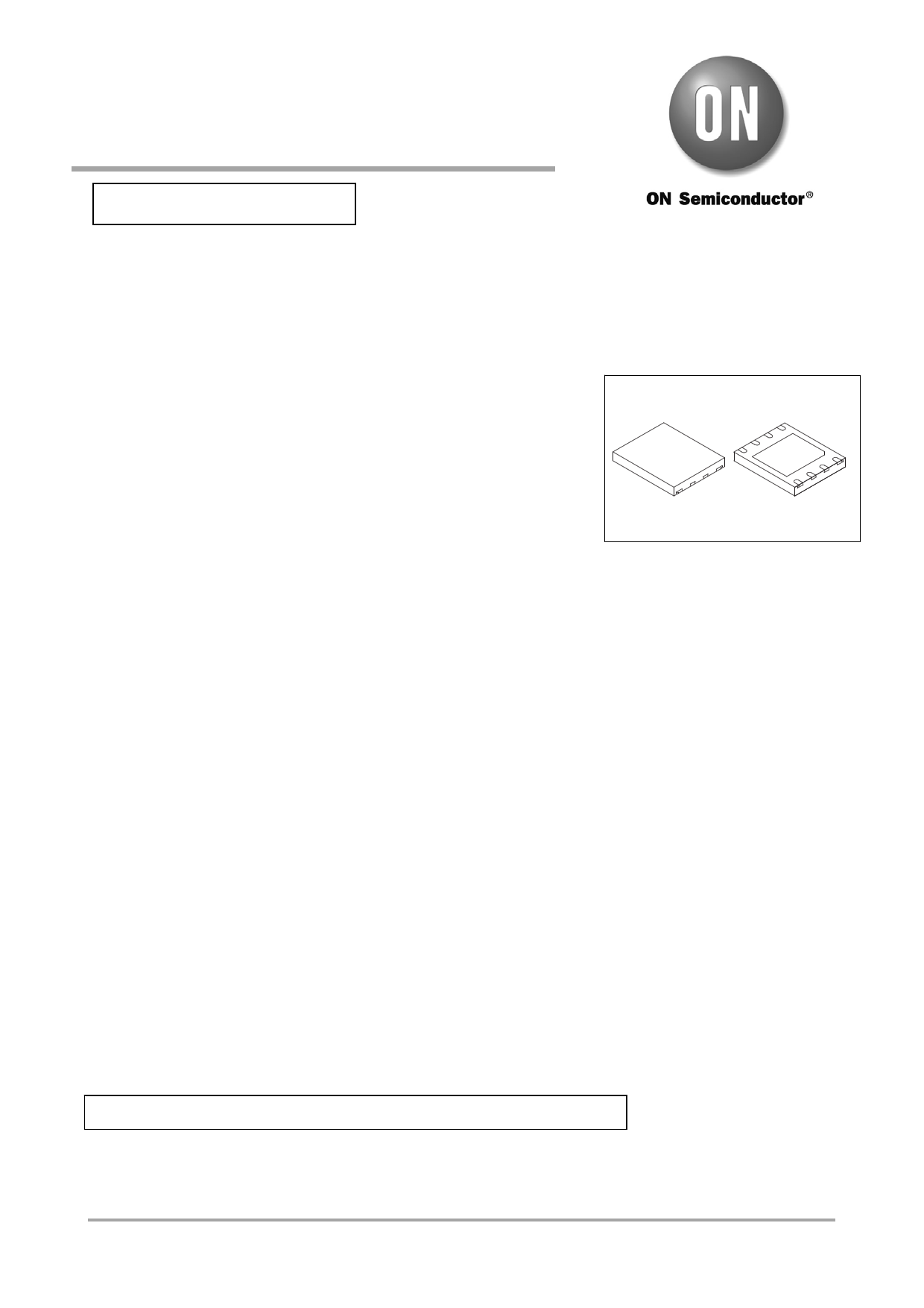
program method of LE25W81QE can program any amount of data from 1 to VDFN8 5x6, 1.27P / VSON8T (6x5)
256 bytes. This IC incorporates ON Semi’s unique high-speed programming
function which enables fast 0.3ms (typ.) page program time.
The program time of 1.5s (typ.) when programming 8-Mbit full-memory space makes for fast data writing when the
chip erase function is used. While making the most of the features inherent to a serial flash memory device, the
LE25W81QE is housed in an 8-pin ultra-miniature package. Serial flash memory devices tend to be at a disadvantage in
terms of their read speed, but the LE25W81QE has maximally eliminated this speed-related disadvantage by supporting
clocks with frequencies up to 50MHz under SPI bus specifications. All these features make this device ideally suited to
storing program codes in applications such as portable information devices and small disk systems, which are required
to have increasingly more compact dimensions.
Features
Read/write operations enabled by single 2.6V power supply : 2.45 to 3.6V supply voltage range
Operating frequency : 30MHz
Temperature range
: –20 to +70C (Read operation)
0 to +70C (Write operation)
Serial interface
: SPI mode 0, mode 3 supported
Sector size
: 4K bytes/small sector, 64K bytes/sector
Small sector erase, sector erase, chip erase functions
Page program function (256 bytes / page)
Block protect function
Highly reliable read/write
Number of rewrite times: 100,000 times
Small sector erase time : 80ms (typ.), 300ms (max.)
Sector erase time
: 100ms (typ.), 400ms (max.)
Chip erase time
: 250ms (typ.), 3.0s (max.)
Page program time : 0.3ms/256 bytes (typ.), 1ms/256 bytes (max.)
Status functions
: Ready/busy information, protect information
Data retention period : 20 years
Package
: VDFN8 56
* This product is licensed from Silicon Storage Technology, Inc. (USA).
This document contains information on a new product. Specifications and information
herein are subject to change without notice.
ORDERING INFORMATION
See detailed ordering and shipping information on page 21 of this data sheet.
© Semiconductor Components Industries, LLC, 2014
November 2014 - Rev. P0
1
Publication Order Number :
LE25W81QE/D
1 page 
LE25W81QE
Device Operation
The LE25W81QE features electrical on-chip erase functions using a single 2.6V power supply, that have been added to
the EPROM functions of the industry standard that support serial interfaces. Interfacing and control are facilitated by
incorporating the command registers inside the chip. The read, erase, program and other required functions of the
device are executed through the command registers. The command addresses and data input in accordance with "Table
2 Command Settings" are latched inside the device in order to execute the required operations. "Figure 3 Serial Input
Timing" shows the timing waveforms of the serial data input. First, at the falling CS edge the device is selected, and
serial input is enabled for the commands, addresses, etc. These inputs are introduced internally in sequence starting with
bit 7 in synchronization with the rising SCK edge. At this time, output pin SO is in the high-impedance state. The
output pin is placed in the low-impedance state when the data is output in sequence starting with bit 7 synchronized to
the falling clock edge during read, status register read and silicon ID. Refer to "Figure 4 Serial Output Timing" for the
serial output timing.
The LE25W81QE supports both serial interface SPI mode 0 and SPI mode 3. At the falling CS edge, SPI mode 0 is
automatically selected if the logic level of SCK is low, and SPI mode 3 is automatically selected if the logic level of
SCK is high.
Figure 3 Serial Input Timing
CS
SCK
SI
SO
tCLS
tCSS
tDS tDH
DATA VALID
High Impedance
tCPH
tCLHI tCLLO tCSH
tCLH
High Impedance
Figure 4 Serial Output Timing
CS
SCK
SO
SI
tCLZ
tHO
DATA VALID
tV
tCHZ
www.onsemi.com
5
5 Page 
LE25W81QE
6. Small Sector Erase
Small sector erase is an operation that sets the memory cell data in any small sector to "1". A small sector consists of
4Kbytes. "Figure 12 Small Sector Erase" shows the timing waveforms, and Figure 21 shows a small sector erase
flowchart. The small sector erase command consists of the first through fourth bus cycles, and it is initiated by inputting
the 24-bit addresses following (D7h or 20h). Addresses A19 to A12 are valid, and Addresses A23 to A20 are "don't
care". After the command has been input, the internal erase operation starts from the rising CS edge, and it ends
automatically by the control exercised by the internal timer. Erase end can also be detected using status register RDY.
Figure 12 Small Sector Erase
CS
Self-timed
Erase Cycle
tSSE
SCK
SI
Mode3 0 1 2 3 4 5 6 7 8
Mode0
15 16 23 24 31
8CLK
D7h or 20h
Add. Add. Add.
High Impedance
SO
7. Sector Erase
Sector erase is an operation that sets the memory cell data in any sector to "1". A sector consists of 64Kbytes. "Figure
13 Sector Erase" shows the timing waveforms, and Figure 21 shows a sector erase flowchart. The sector erase command
consists of the first through fourth bus cycles, and it is initiated by inputting the 24-bit addresses following (D8h).
Addresses A19 to A16 are valid, and Addresses A23 to A20 are "don't care". After the command has been input, the
internal erase operation starts from the rising CS edge, and it ends automatically by the control exercised by the internal
timer. Erase end can also be detected using status register RDY.
Figure 13 Sector Erase
CS
Self-timed
Erase Cycle
tSE
SCK
SI
Mode3
Mode0
012345678
15 16 23 24 31
8CLK
D8h Add. Add. Add.
High Impedance
SO
www.onsemi.com
11
11 Page | ||
| Páginas | Total 21 Páginas | |
| PDF Descargar | [ Datasheet LE25W81QE.PDF ] | |
Hoja de datos destacado
| Número de pieza | Descripción | Fabricantes |
| LE25W81QE | 8M-bit (1024K x 8) Serial Flash Memory | ON Semiconductor |
| Número de pieza | Descripción | Fabricantes |
| SLA6805M | High Voltage 3 phase Motor Driver IC. |
Sanken |
| SDC1742 | 12- and 14-Bit Hybrid Synchro / Resolver-to-Digital Converters. |
Analog Devices |
|
DataSheet.es es una pagina web que funciona como un repositorio de manuales o hoja de datos de muchos de los productos más populares, |
| DataSheet.es | 2020 | Privacy Policy | Contacto | Buscar |