|
|
PDF QN9021 Data sheet ( Hoja de datos )
| Número de pieza | QN9021 | |
| Descripción | Ultra Low Power BLE System-on-Chip Solution | |
| Fabricantes | NXP Semiconductors | |
| Logotipo | ||
Hay una vista previa y un enlace de descarga de QN9021 (archivo pdf) en la parte inferior de esta página. Total 30 Páginas | ||
|
No Preview Available !
QN902X
Ultra Low Power BLE System-on-Chip Solution
Rev. 1.1 — 10 February 2015
Product data sheet
1. Introduction
QN902x is an ultra-low power wireless System-on-Chip (SoC) for Bluetooth Smart
applications, supporting both master and slave modes. It integrates a high performance
2.4 GHz RF transceiver with a 32-bit ARM Cortex-M0 MCU, Flash memory, and analog
and digital peripherals.
By integrating a Bluetooth v4.0 Low Energy compliant radio, link controller and host
stack, QN902x provides a single chip solution for Bluetooth Smart applications. The 32-
bit ARM Cortex-M0 MCU and on-chip memory provide additional signal processing and
room to run applications for a true single-chip Bluetooth Smart solution. In addition,
QN902x can also be utilized as a network processor by connecting to an application
processor via UART or SPI to add Bluetooth Smart feature to any products.
QN902x comes with complete analog peripherals and digital interfaces to enable easy
connection to any analog or digital peripherals or sensors, and external application
processor in network processor mode.
2. General description
QN902x is an ultra-low power, high performance and highly integrated Bluetooth v4.0
Low Energy (BLE) solution for Bluetooth Smart applications such as sports/fitness,
human interface devices, and app-enabled smart accessories. It is especially designed
for wearable electronics and can run on small capacity battery such as a coin cell battery.
QN902x integrates a BLE radio, controller, protocol stack and profile software on a single
chip, providing a flexible and easy to use BLE SoC solution. It also includes a high
performance MCU and on-chip memory that can support users to develop a single-chip
wireless MCU solution. Users can also utilize QN902x as a network processor by
connecting to an application processor for more advanced applications.
Additional system features include fully integrated DC/DC and LDO, low power sleep
timer, battery monitor, general purpose ADC, and GPIOs, to further reduce overall
system cost and size. QN902x operates with a power supply range of
2.4 V to 3.6 V and has very low power consumption in all modes, enabling long lifetimes
in battery-operated systems while maintaining excellent RF performance.
1 page 
NXP Semiconductors
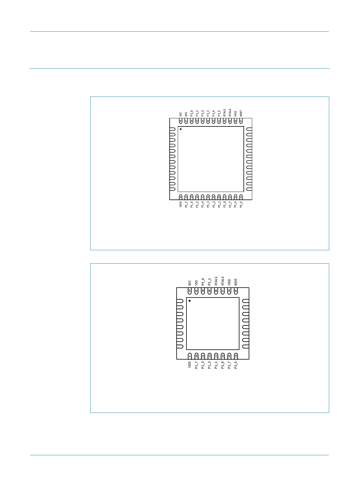
7. Pinning information for QN902x
7.1 Pinning
QN902X
Ultra Low Power BLE System-on-Chip Solution
VCC 1
P0_7 2
P0_6 3
XTAL2_32K 4
XTAL1_32K 5
P0_5 6
P0_4 7
P0_3 8
P0_2 9
P0_1 10
P0_0 11
VSS 12
QN9020
QFN48
(6x6 mm)
36 VDD
35 VSS
34 RFP
33 RFN
32 RVDD
31 RSTN
30 P3_6
29 P2_0
28 P2_1
27 P2_2
26 P2_3
25 P2_4
Fig 2.
QN9020 is in a 6x6 mm QFN48 package. The back plate must be grounded to the application
PCB in order to achieve optimal performance.
QN9020 Pin configuration
VCC
P0_7
P0_6
XTAL2_32K
XTAL1_32K
P0_3
P0_0
VSS
1
2
3
4
5
6
7
8
QN9021
QFN32
(5x5 mm)
24 VDD
23 VSS
22 RFP
21 RFN
20 RVDD
19 RSTN
18 P2_3
17 P2_4
Fig 3.
QN9021 is in a 5x5 mm QFN32 package. The back plate must be grounded to the application
PCB in order to achieve optimal performance.
QN9021 Pin configuration
QN902X
Product data sheet
All information provided in this document is subject to legal disclaimers.
Rev. 1.1 — 10 February 2015
© NXP Semiconductors N.V. 2015. All rights reserved.
5 of 35
5 Page 
NXP Semiconductors
QN902X
Ultra Low Power BLE System-on-Chip Solution
0xFFFFFFFF
Reserved
0xEFFFFFFF
MCU private peripherals
0xE0000000
Reserved
ADC
0x50013FFF
0x50010000
Reserved
GPIO
0x50003FFF
0x50000000
Reserved
0x400EFFFF
APB peripherals
0x40000000
Reserved
0x1000FFFF
System memory
0x10000000
ROM
0x00000000
Fig 4. Memory address map
8.1.3 RESET generation
The device has four reset sources. The following events generate a reset:
Forcing RSTN pin low
Power-on reset
Brown-out reset
Watchdog timeout reset
8.1.4 Nested Vectored Interrupt Controller (NVIC)
QN9020 supports Cortext-M0 built-in Nested Vectored Interrupt Controller (NVIC) with 24
external interrupt inputs. External interrupt signals connect to the NVIC, and the NVIC
prioritizes the interrupts. Software can set the priority of each interrupt. The NVIC and
Cortex-M0 processor core are closely coupled, providing low-latency interrupt processing
and efficient processing of late arriving interrupts.
8.1.5 Clock and power management
QN902x provides flexible clocking scheme to balance between performance and power.
A high frequency crystal oscillator is utilized to provide reference frequency and system
clock, which supports 16/32 MHz external crystal with ±50 ppm accuracy. The system
clock could be 32 MHz or its divided versions.
QN902X
Product data sheet
All information provided in this document is subject to legal disclaimers.
Rev. 1.1 — 10 February 2015
© NXP Semiconductors N.V. 2015. All rights reserved.
11 of 35
11 Page | ||
| Páginas | Total 30 Páginas | |
| PDF Descargar | [ Datasheet QN9021.PDF ] | |
Hoja de datos destacado
| Número de pieza | Descripción | Fabricantes |
| QN9020 | Ultra Low Power BLE System-on-Chip Solution | NXP Semiconductors |
| QN9021 | Ultra Low Power BLE System-on-Chip Solution | NXP Semiconductors |
| Número de pieza | Descripción | Fabricantes |
| SLA6805M | High Voltage 3 phase Motor Driver IC. |
Sanken |
| SDC1742 | 12- and 14-Bit Hybrid Synchro / Resolver-to-Digital Converters. |
Analog Devices |
|
DataSheet.es es una pagina web que funciona como un repositorio de manuales o hoja de datos de muchos de los productos más populares, |
| DataSheet.es | 2020 | Privacy Policy | Contacto | Buscar |
