|
|
|
PDF L6000 Data sheet ( Hoja de datos )
| Número de pieza | L6000 | |
| Descripción | SINGLE CHIP READ & WRITE CHANNEL | |
| Fabricantes | STMicroelectronics | |
| Logotipo | ||
Hay una vista previa y un enlace de descarga de L6000 (archivo pdf) en la parte inferior de esta página. Total 24 Páginas | ||
|
No Preview Available !
L6000
SINGLE CHIP READ & WRITE CHANNEL
ADVANCE DATA
SUPPORTS 9-32Mbit/s DATA RATE OPERA-
TION IN RLL [1,7] CONSTRAINT
- Data Rate is Programmable
SUPPORTS ZONED BIT RECORDING AP-
PLICATIONS
LOW POWER OPERATION (500mW TYPI-
CAL @ 5V @ 32Mbits/Sec
PROVIDES PROGRAMMABILITY THROUGH
SERIAL MICROPROCESSOR INTERFACE
AND INTERNAL REGISTERS
- Bi-directional access to internal registers of
pulse detector, filter, servo demodulator,
frequency synthesizer and data separator.
PROGRAMMABLE POWER DOWN MODES
Full power-down mode (5mW max.)
POWER SUPPLY RANGE 4.3 to 5.5V
DESCRIPTION
The L6000 is a 5V single chip read channel IC. It
contains all the functions needed to implement a
high performance read channel including the
TQFP64
(10 x 10)
ORDERING NUMBER: L6000
OPERATING TEMPERATURE: 0°C to 70°C
pulse detector, programmable active filter, servo
demodulator, frequency sinthesizer, and data
separator, at data rates up to 32 Mbit/s. A single
external resistor sets the reference current for the
internal DAC which, in turn, fixes the data rate.
This device is programmed through a serial port
and banks of internal registers. It is fully compat-
ible with zoned bit recording applications. Exter-
nal components do not need to be changed when
switching between zones. The L6000 is manufac-
tured using an advanced BiCMOS technology.
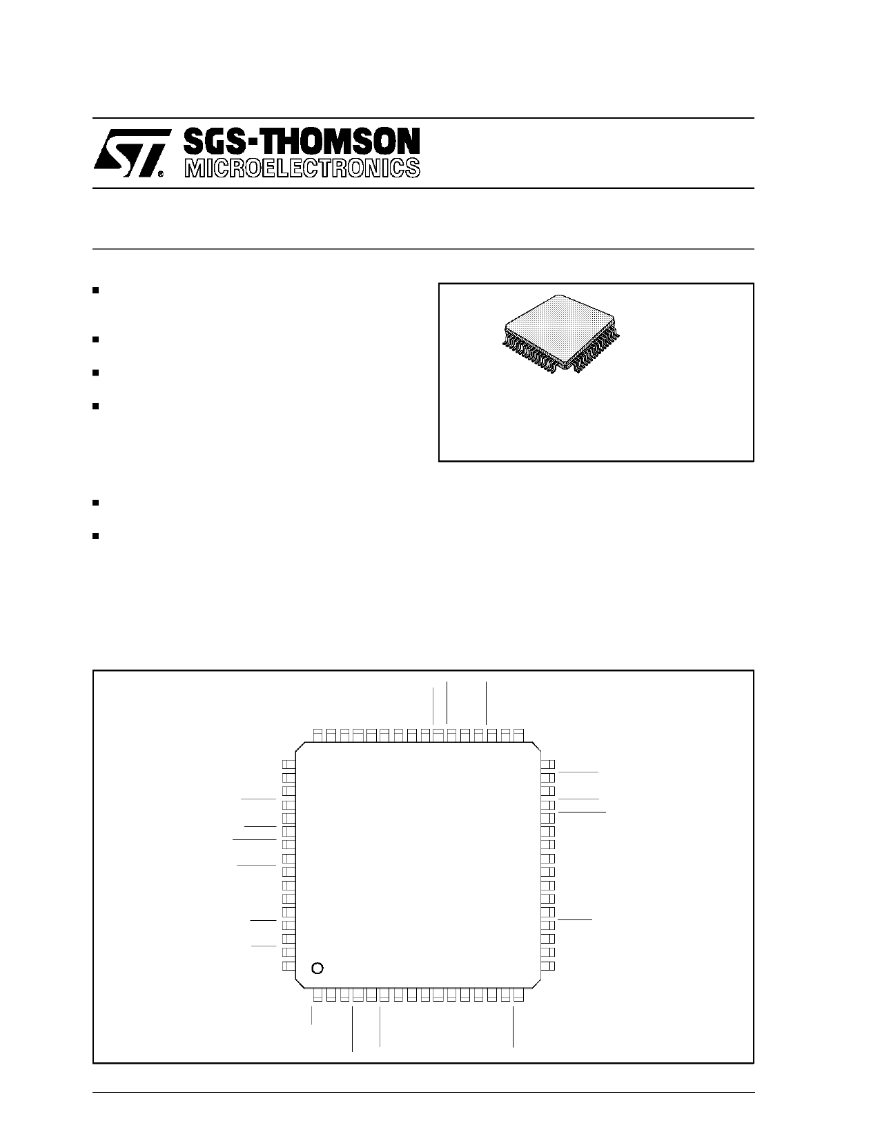
PIN CONNECTION (Top view)
LEVEL
LEVEL REF V
CLOC K PATH
CLOC K PATH
DATA PATH
DATA PATH
FI LT NORM OUT
FI LT NORM OUT
FI LT DIFF OUT
FI LT DIFF OUT
VCC PULSE DET
FILT ER IN
FILT ER IN
PTAT R
AGC O UT
AGC O UT
48 47 46 45 44 43 42 41 40 39 38 37 36 35 34 33
49 32
50 31
51 30
52 29
53 28
54 27
55 26
56 25
57 24
58 23
59 22
60 21
61 20
62 19
63 18
64 17
1 2 3 4 5 6 7 8 9 10 11 12 13 14 15 16
DATA SEP FLT
DATA SEP FLT
VCC DATA SEP
READ DATA I/O
ADDR MARK DET
READ REF CLOC K
WRIT E CLOC K
MULT T P1
MULT T P2
GND I/O
WRIT E DATA NR2 IN
READ NR2 O UTPUT
WRIT E DATA
VCC I/O
WRIT E GATE
READ GATE
M9 2L6000- 01
August 1993
1/24
This is advanced information on a new product now in development or undergoing evaluation. Details are subject to change without notice.
1 page 
L6000
PIN DESCRIPTION (continued)
Pin #
Symbol
OUTPUT
64, 63
AGC OUT,
AGC OUT
29 READ DATA I/O
Type
O
I/O
46 POSITION OUT O
56, 55
58, 57
28
FILT NORM OUT,
FILT NORM OUT
FILT DIFF OUT,
FILT DIFF OUT
ADDR MARK DET
O
O
O
25 MULT TP1 O
21 READ NRZ O
OUTPUT
27 READ REF CLOCK 0
24 MULT TP2 O
20 WRITE DATA O
13 FREQ OUT TP O
Description
AGC AMPLIFIER OUTPUT: Differential AGC amplifier output pins.
READ DATA I/O: Bi-directional TTL pin. Output is active in the servo mode or
when both READ GATE and WRITE GATE are deasserted. In test mode, this
is a TTL input used to drive the data separator. The TTL input is enabled by
setting RDI in the control register CB.
POSITION ERROR SIGNAL: A Position error signal of A minus B output which
is referenced to SERVO REF V.
FILTER DIFFERENTIAL NORMAL OUTPUTS: Low pass & boosted filter
output signals. Must be AC coupled to the next stage nominally DATA PATH.
FILTER DIFFERENTIAL DIFFERENTIADED OUTPUTS: Differentiated filter
outputs should be AC coupled to the next stage nominally CLOCK PATH.
ADDRESS MARK DETECT: Tristate output pin with TTL output levels. It is in
its high impedance state when WRITE GATE is asserted. When READ GATE
is asserted and the register bit is set for soft sector, an address mark search is
initiated in the soft sector operation. This output is latched low (true) when an
address mark has been detected. Deasserting pin READ GATE deasserts pin
ADDR MARK DET.
MULTIPLEXED TEST POINT OUTPUT: An open emitter ECL output test point.
The test point output is enabled by Setting ED in the control registerCB. The
controlling signal is PD_TEST in the control register CA. When PD_TEST is low ,
the test point output is the delayed read data DRD. The posistive edges of this
signal indicate the data bit position. The positive edges of the DRD and VCOREF
outputs can be used to estimate window centering. The time jitter of DRD’s
positive edge is an indication of media bit jitter. When PD_TEST is high the test
point out is the comparator of the pulse qualifier. The positive edge indicates that
the input signal has exceeded the positive threshold while a negative edge
indicates that the input signal has gone below the negative threshold. Two external
resistors are required to use this pin. They should be removed during normal
operation to reduce power dissipation.
NRZ OUTPUT DATA: Tristate ouput pin with TTL output levels. It is in its high
impedance state when READ GATE is deasserted. Read data output when
READ GATE is asserted.
READ REFERENCE CLOCK: TTL output. A multiplexed clock source used by
the controller, see Clocks and Modes. During a mode change, no glitches are
generated and no more than one lost clock pulse will occur. READ REF
CLOCK remains Fout/3 after READ GATE is asserted, until after synchronized
bits are detected.
MULTIPLEXED TEST POINT OUTPUT: An open emitter ECL output test point.
This test point output is enabled by using the same control bit enabling the
MULT TP1 output. When the controlling signal, PD_TEST is desserted, the test
point output is the VCO reference input (VCOREF) to the phase detector. The
positive edges are phase locked to Delayed Read Data (DRD). The negative
edges of this open emitter output signal indicate the edges of the decode
window. When PD_TEST is high, the test point output represents the state of
the clock comparator in the pulse qualifier. The signal transitions indicate zero
crossing of the differentiated signal from the electronic filter. Two external
resistor are required to use this pin. They should be removed during normal
operation to reduce power dissipation.
WRITE DATA: TTL output. Encoded write data output. The data is
automatically resynchronized (independent of the delay between READ REF
CLOCK and WRITE CLOCK) to the reference clock FSout. Falling edge of the
WRITE DATA is the data edge.
REFERENCE FREQUENCY OUTPUT: An open emitter ECL output test point.
The frequency is the frequency synthesizer output frequency. This output is
enabled by control register CA. Two external resistors are required to use this
pin. They should be removed during normal operation to reduce power
dissipation.
5/24
5 Page 
L6000
PULSE DETECTOR AND SERVO DEMODULATOR CHARACTERISTICS (continued)
Symbol
Id
ILKG
ILKG
K4
K5
Tper
T1
Th
Tf
Tr
Parameter
HOLD CAP A/B Disch. Current
HOLD CAP A/B Leakage Cur.
SERVO BYP Pin Leakage Cur.
SERVO BYP Pin
Charge/Discharge Current
Maximum SERVO BYP Pin
Charge Current
READ DATA I/O Output Pulse
Period
READ DATA I/O Output Pulse
Low Time
READ DATA I/O Output Pulse
High Time
READ DATA I/O Output Pulse
Fail Time
READ DATA I/O Output Pulse
Rise Time
Test Condition
Absolute value
HOLDS = Low
Ibyps = K4 ⋅ [K5 -
DATAPATHApp –
DATAPATHBpp]
CL ≤ 15pF
RDIO ≤ 0.8V
RDIO ≥ 0.8V
CL ≤ 15pF, 2.0V to 0.8V
CL ≤ 15pF, 0.8V to 2.0V
Min.
0.8
–
–
450
0.70
Typ.
1.5
–
–
640
1.00
Max.
2.2
±0.5
±0.2
880
Unit
mA
µA
µA
µA/Vpp
1.30 V/V
190 300 490
50 –
–
9 23 33
29 –
–
––5
––8
µA
ns
ns
ns
ns
ns
PROGRAMMABLE FILTER CHARACTERISTICS
Symbol
Parameter
Test Condition
Min. Typ. Max.
Test Condition s: Vccn = 5V + 10% - 14%, Tamb = 0 to 70°C, Tj = 25 to 125°C, unless otherwise specified.
The input signals are AC coupled to FILTER and FIL TER IN. C ≥ 22nF.
FC Filter Cutoff Frequency,
f at -3dB point
FC = 0.141732MHz *FCDAC,
42 ≤ FCDAC ≤ 127, FCDAC is
value of frequency DAC
6
– 18
FCA
Filter fc Accuracy
FCDAC = 127
– 10 – +10
AN FILT NORM OUT Differential Gain f = 0.67FC, FBDAC = 0
1.6 2 2.4
AD FILT DIFF OUT Differential Gain
0.9AN – 1.1AN
FB Frequency Boost @ FC
FB (dB) = 20log [0.0273
– 13 –
(FBDAC)+1], 0 ≤ FBDAC ≤ 127
FBDAC = 127
@6dB; FBDAC = 36
@13dB; FBDAC = 127
– 0.75 – + 0.75
–2.0 +2.0
TGDO
Group Delay Variation without
Boost
FC = 6MHz to 18MHz,
f = 0.2FC to FC FBDAC = 0
–3 – +3
FC = 6MHz to 18MHz,
–4 – +4
FBDAC = 0, f = FC to 1.75FC
TGDB
Group Delay Variation with
Maximum Boost
FC = 6 to 18MHz,
– 3 – +3
f = 0.2 FC to FC, FBDAC = 127
FC = 6MHz to 18MHz,
– 4 – +4
FBDAC = 127, f = FC to 1.75FC
VIF Filter Differential Input Dynamic THD = 1% max, f = 0.67FC,
Range
FBDAC = 0
0.5 –
–
THD = 2% max, f = 0.67FC,
FBDAC = 0
0.75 –
–
RIN Filter Diff. Input resistance
5.0 –
–
RIZ Filter Diff. Input Resistance with Low – Z mode
Shorted Inputs
100 300 500
CIN Filter Diff. Input Capacitance
––7
Unit
MHz
%
V/V
V/V
dB
dB
dB
%
(2)
%
(2)
%
(2)
%
(2)
Vpp
Vpp
KΩ
Ω
pF
(2) Test limits under evaluation.
11/24
11 Page | ||
| Páginas | Total 24 Páginas | |
| PDF Descargar | [ Datasheet L6000.PDF ] | |
Hoja de datos destacado
| Número de pieza | Descripción | Fabricantes |
| L6000 | SINGLE CHIP READ & WRITE CHANNEL | STMicroelectronics |
| L6002 | LEDs | Hamamatsu Photonic Systems |
| L6004Dx | Sensitive Triacs | Teccor Electronics |
| L6008 | Sensitive Triacs | Teccor Electronics |
| Número de pieza | Descripción | Fabricantes |
| SLA6805M | High Voltage 3 phase Motor Driver IC. |
Sanken |
| SDC1742 | 12- and 14-Bit Hybrid Synchro / Resolver-to-Digital Converters. |
Analog Devices |
|
DataSheet.es es una pagina web que funciona como un repositorio de manuales o hoja de datos de muchos de los productos más populares, |
| DataSheet.es | 2020 | Privacy Policy | Contacto | Buscar |