|
|
|
PDF ADRF6702 Data sheet ( Hoja de datos )
| Número de pieza | ADRF6702 | |
| Descripción | 1200 MHz to 2400 MHz Quadrature Modulator | |
| Fabricantes | Analog Devices | |
| Logotipo | ||
Hay una vista previa y un enlace de descarga de ADRF6702 (archivo pdf) en la parte inferior de esta página. Total 30 Páginas | ||
|
No Preview Available !
Data Sheet
1200 MHz to 2400 MHz Quadrature Modulator with
1550 MHz to 2150 MHz Frac-N PLL and Integrated VCO
ADRF6702
FEATURES
IQ modulator with integrated fractional-N PLL
Output frequency range: 1200 MHz to 2400 MHz
Internal LO frequency range: 1550 MHz to 2150 MHz
Output P1dB: 13.1 dBm @ 2140 MHz
Output IP3: 29.1 dBm @ 2140 MHz
Noise floor: −159.6 dBm/Hz @ 1960 MHz
Baseband bandwidth: 750 MHz (3 dB)
SPI serial interface for PLL programming
Integrated LDOs and LO buffer
Power supply: 5 V/240 mA
40-lead 6 mm × 6 mm LFCSP
APPLICATIONS
Cellular communications systems
GSM/EDGE, CDMA2000, W-CDMA, TD-SCDMA, LTE
Broadband wireless access systems
Satellite modems
GENERAL DESCRIPTION
The ADRF6702 provides a quadrature modulator and
synthesizer solution within a small 6 mm × 6 mm footprint
while requiring minimal external components.
The ADRF6702 is designed for RF outputs from 1200 MHz to
2400 MHz. The low phase noise VCO and high performance
quadrature modulator make the ADRF6702 suitable for next
generation communication systems requiring high signal
dynamic range and linearity. The integration of the IQ
modulator, PLL, and VCO provides for significant board
savings and reduces the BOM and design complexity.
The integrated fractional-N PLL/synthesizer generates a 2× fLO
input to the IQ modulator. The phase detector together with an
external loop filter is used to control the VCO output. The VCO
output is applied to a quadrature divider. To reduce spurious
components, a sigma-delta (Σ-Δ) modulator controls the
programmable PLL divider.
The IQ modulator has wideband differential I and Q inputs,
which support baseband as well as complex IF architectures.
The single-ended modulator output is designed to drive a
50 Ω load impedance and can be disabled.
The ADRF6702 is fabricated using an advanced silicon-
germanium BiCMOS process. It is available in a 40-lead,
exposed-paddle, Pb-free, 6 mm × 6 mm LFCSP package.
Performance is specified from −40°C to +85°C. A lead-free
evaluation board is available.
Table 1.
Part No.
ADRF6701
ADRF6702
ADRF6703
ADRF6704
Internal LO Range
750 MHz
1150 MHz
1550 MHz
2150 MHz
2100 MHz
2600 MHz
2500 MHz
290 MHz
±3 dB RFOUT Balun Range
400 MHz
1250 MHz
1200 MHz
2400 MHz
1550 MHz
2650 MHz
2050 MHz
3000 MHz
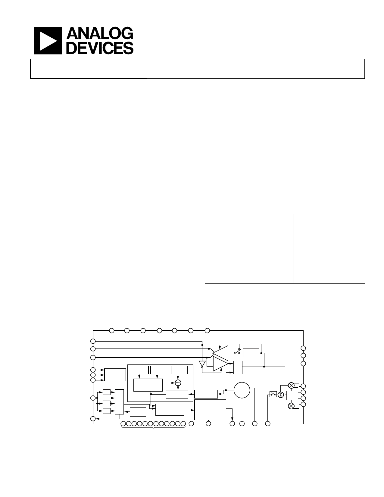
FUNCTIONAL BLOCK DIAGRAM
VCC7 VCC6 VCC5 VCC4 VCC3 VCC2 VCC1
34 29 27 22 17 10
1
LOSEL 36
ADRF6702
LON 37
LOP 38
BUFFER
DIVIDER
÷2
40 DECL3
9 DECL2
BUFFER
DATA 12
CLK 13
LE 14
REFIN 6
MUXOUT 8
SPI
INTERFACE
×2
MUX
÷2
÷4
FRACTION
REG
MODULUS
INTEGER
REG
THIRD-ORDER
FRACTIONAL
INTERPOLATOR
N COUNTER
21 TO 123
TEMP
SENSOR
–
+
PHASE
FREQUENCY
DETECTOR
PRESCALER
÷2
CHARGE PUMP
250µA,
500µA (DEFAULT),
750µA,
1000µA
4 7 11 15 20 21 23 25 28 30 31 35 24
5
GND
NOTES
1. NC = NO CONNECT. DO NOT CONNECT TO THIS PIN.
NC RSET
Figure 1.
2:1
MUX
VCO
CORE
3 39 16 26
CP VTUNE ENOP RFOUT
2 DECL1
÷2
0/90
18 QP
19 QN
32 IN
33 IP
Rev. B
Information furnished by Analog Devices is believed to be accurate and reliable. However, no
responsibility is assumed by Analog Devices for its use, nor for any infringements of patents or other
rights of third parties that may result from its use. Specifications subject to change without notice. No
license is granted by implication or otherwise under any patent or patent rights of Analog Devices.
Trademarksandregisteredtrademarksarethepropertyoftheirrespectiveowners.
One Technology Way, P.O. Box 9106, Norwood, MA 02062-9106, U.S.A.
Tel: 781.329.4700
www.analog.com
Fax: 781.461.3113
©2011 Analog Devices, Inc. All rights reserved.
1 page 
Data Sheet
ADRF6702
Parameter
BASEBAND INPUTS
I and Q Input DC Bias Level
Bandwidth
Differential Input Impedance
Differential Input Capacitance
LOGIC INPUTS
Input High Voltage, VINH
Input Low Voltage, VINL
Input Current, IINH/IINL
Input Capacitance, CIN
TEMPERATURE SENSOR
Output Voltage
Temperature Coefficient
POWER SUPPLIES
Voltage Range
Supply Current
Test Conditions/Comments
IP, IN, QP, QN pins
POUT ≈ −7 dBm, RF flatness of IQ modulator output calibrated out
0.5 dB
3 dB
CLK, DATA, LE, ENOP, LOSEL
VPTAT voltage measured at MUXOUT
TA = 25°C, RL ≥10 kΩ (LO buffer disabled)
TA = −40°C to +85°C, RL ≥10 kΩ
VCC1, VCC2, VCC3, VCC4, VCC5, VCC6, VCC7
Normal Tx mode (PLL and IQMOD enabled, LO buffer disabled)
Tx mode using external LO input (internal VCO/PLL disabled)
Tx mode with LO buffer enabled
Power-down mode
Min Typ
400 500
350
750
920
1
1.4
0
0.1
5
1.64
3.9
4.75 5
240
130
290
22
Max Unit
600 mV
MHz
MHz
Ω
pF
3.3 V
0.7 V
μA
pF
V
mV/°C
5.25 V
mA
mA
mA
μA
1 The figure of merit (FOM) is computed as phase noise (dBc/Hz) – 10log10(fPFD) – 20log10(fLO/fPFD). The FOM was measured across the full LO range, with fREF = 80 MHz,
fREF power = 10 dBm (500 V/μs slew rate) with a 40 MHz fPFD. The FOM was computed at 50 kHz offset.
Rev. B | Page 5 of 36
5 Page 
Data Sheet
0
–10
TTTAAA
=
=
=
–40°C
+25°C
+85°C
–20
–30
–40
–50
–60
–70
–80
1550 1600 1650 1700 1750 1800 1850 1900 1950 2000 2050 2100 2150
LO FREQUENCY (MHz)
Figure 10. Carrier Feedthrough vs. LO Frequency (fLO) and Temperature;
Multiple Devices Shown
0
–10
TTTAAA
=
=
=
–40°C
+25°C
+85°C
–20
–30
–40
–50
–60
–70
–80
–90
1550 1600 1650 1700 1750 1800 1850 1900 1950 2000 2050 2100 2150
LO FREQUENCY (MHz)
Figure 11. Sideband Suppression vs. LO Frequency (fLO) and Temperature;
Multiple Devices Shown
90
80
OIP2
70
60
50
40
OIP3
30
20
10
0
TTTAAA
=
=
=
–40°C
+25°C
+85°C
1550 1600 1650 1700 1750 1800 1850 1900 1950 2000 2050 2100 2150
LO FREQUENCY (MHz)
Figure 12. OIP3 and OIP2 vs. LO Frequency (fLO) and Temperature
(POUT ≈ −2 dBm per Tone); Multiple Devices Shown
ADRF6702
0
–10
TTTAAA
=
=
=
–40°C
+25°C
+85°C
–20
–30
–40
–50
–60
–70
–80
1550 1600 1650 1700 1750 1800 1850 1900 1950 2000 2050 2100 2150
LO FREQUENCY (MHz)
Figure 13. Carrier Feedthrough vs. LO Frequency (fLO) and Temperature After
Nulling at 25°C; Multiple Devices Shown
0
–10
TTTAAA
=
=
=
–40°C
+25°C
+85°C
–20
–30
–40
–50
–60
–70
–80
–90
1550 1600 1650 1700 1750 1800 1850 1900 1950 2000 2050 2100 2150
LO FREQUENCY (MHz)
Figure 14. Sideband Suppression vs. LO Frequency (fLO) and Temperature
After Nulling at 25°C; Multiple Devices Shown
–20 TA = –40°C
–25 TA = +25°C
–30 TA = +85°C
–35
–40 THIRD-ORDER DISTORTION
–45
–50
–55
–60
–65
–70
–75
SECOND-ORDER DISTORTION
–80
1550 1600 1650 1700 1750 1800 1850 1900 1950 2000 2050 2100 2150
LO FREQUENCY (MHz)
Figure 15. Second- and Third-Order Distortion vs. LO Frequency (fLO) and
Temperature
Rev. B | Page 11 of 36
11 Page | ||
| Páginas | Total 30 Páginas | |
| PDF Descargar | [ Datasheet ADRF6702.PDF ] | |
Hoja de datos destacado
| Número de pieza | Descripción | Fabricantes |
| ADRF6701 | 400 MHz to 1250 MHz Quadrature Modulator | Analog Devices |
| ADRF6702 | 1200 MHz to 2400 MHz Quadrature Modulator | Analog Devices |
| ADRF6703 | 1550 MHz to 2650 MHz Quadrature Modulator | Analog Devices |
| ADRF6704 | 2050 MHz to 3000 MHz Quadrature Modulator | Analog Devices |
| Número de pieza | Descripción | Fabricantes |
| SLA6805M | High Voltage 3 phase Motor Driver IC. |
Sanken |
| SDC1742 | 12- and 14-Bit Hybrid Synchro / Resolver-to-Digital Converters. |
Analog Devices |
|
DataSheet.es es una pagina web que funciona como un repositorio de manuales o hoja de datos de muchos de los productos más populares, |
| DataSheet.es | 2020 | Privacy Policy | Contacto | Buscar |