|
|
|
PDF 78M6612 Data sheet ( Hoja de datos )
| Número de pieza | 78M6612 | |
| Descripción | Dual-Outlet Power and Energy Measurement IC | |
| Fabricantes | TERIDIAN Semiconductor | |
| Logotipo | ||
Hay una vista previa y un enlace de descarga de 78M6612 (archivo pdf) en la parte inferior de esta página. Total 70 Páginas | ||
|
No Preview Available !
78M6612www.DataSheet4U.com
Single-Phase, Dual-Outlet
Power and Energy Measurement IC
Simplifying System IntegrationTM
DATA SHEET
June 2009
DESCRIPTION
The Teridian 78M6612 is a highly integrated,
single-phase, power and energy measurement and
monitoring SOC which includes a 32-bit compute engine
(CE), an MPU core, RTC, and Flash. The Teridian
patented Single
Converter Technology® with a 22-bit delta-sigma ADC, 4
analog inputs, digital temperature compensation, and
precision voltage reference supports a wide range of
single-phase, dual-outlet power measurement applications
with very few external components.
With measurement technology leveraged from Teridian’s
flagship utility metering IC’s it offers features including
32 KB of Flash program memory, 2 KB shared RAM, three
low power modes with internal timer or external event wake-
up, 2 UARTs , I2C/Micro wire EEPROM I/F, and an in-
system programmable Flash. Complete Outlet
Measurement Unit (OMU) and AC Power Monitor
(AC-PMON) firmware is available or can be pre-loaded into
the IC.
A complete array of ICE and development tools,
programming libraries and reference designs enable rapid
development and certification of Power and Energy
Measurement solutions that meet the most demanding
worldwide electricity metering standards.
LIVE
NEUT
CT
OUTLET
POWER SUPPLY
POWER
FAULT
32 kHz
CONVERTER
IA
VA
IB
VB
VOLTAGE REF
VREF
VBIAS
SERIAL PORTS
TX0
RX0
RX1
TX1
COMPARATOR
V1
OSC/PLL
XIN
XOUT
V3.3A
V3.3
SYS
TERIDIAN
78M6612
TEMP
SENSOR
GNDA GNDD
PWR MODE
CONTROL
WAKE-UP
REGULATOR
VBAT
V2.5
DIO, PULSE
RAM
FLASH
COMPUTE
ENGINE
COM0..3
SEG0..18
SEG 24..31/
DIO 4..11
SEG 34..37/
DIO 14..17
MPU
RTC
TIMERS
SEG 32,33,
38/ICE
ICE ICE_E
OPTIONAL
BATTERY
OPTIONAL
I2 C or µWire
EEPROM
V3P3D
GNDD
FEATURES
• Measures each outlet of a duplex receptacle with a
single IC
• Provides complete energy measurement and
communication protocol capability in a single IC
• Intelligent switch control capability
• < 0.5% Wh accuracy over 2000:1 current range
and over temperature
• Exceeds IEC62053 / ANSIC12.20 standards
• Voltage reference < 40 ppm/°C
• Four sensor inputs – VDD referenced
• Low jitter Wh and VARh pulse test outputs (10 kHz
maximum)
• Pulse count for pulse outputs
• Line frequency count for RTC
• Digital temperature compensation
• Sag detection for phase A and B
• Independent 32-bit compute engine
• 46-64 Hz line frequency range with same
calibration
• Phase compensation (±7°)
• Battery backup for RTC and battery monitor
• Three battery modes with wake-up timer:
Brownout mode (48 µA)
LCD mode (5.7 µA)
Sleep mode (2.9 µA)
• Energy display on main power failure
• Wake-up timer
• 22-bit delta-sigma ADC
• 8-bit MPU (80515), 1 clock cycle per instruction w/
integrated ICE for MPU debug
• RTC with temperature compensation
• Auto-Calibration
• Hardware watchdog timer, power fail monitor
• LCD driver (up to 152 pixels)
• Up to 18 general purpose I/O pins
• 32 kHz time base
• 32 KB Flash with security
• 2 KB MPU XRAM
• Two UARTs
• Digital I/O pins compatible with 5 V inputs
• 64-pin LQFP or 68-pin QFN package
• RoHS compliant (6/6) lead-free packages
• Complete Application Firmware available
Rev. 1.2
© 2009 Teridian Semiconductor Corporation
1
1 page 
DS_6612_001
78M66w1w2wD.DaattaaShSeeht4eUe.ctom
Figures
Figure 1: IC Functional Block Diagram.....................................................................................................7
Figure 2: General Topology of a Chopped Amplifier ...............................................................................10
Figure 3: AFE Block Diagram ................................................................................................................11
Figure 4: Samples from Multiplexer Cycle ..............................................................................................14
Figure 5: Accumulation Interval..............................................................................................................15
Figure 6: Interrupt Structure...................................................................................................................39
Figure 7: Optical Interface......................................................................................................................42
Figure 8: Connecting an External Load to DIO Pins ...............................................................................44
Figure 9: 3-Wire Interface. Write Command, HiZ=0 ..............................................................................47
Figure 10: 3-Wire Interface. Write Command, HiZ=1 ............................................................................48
Figure 11: 3-Wire Interface. Read Command........................................................................................48
Figure 12: 3-Wire Interface. Write Command when CNT=0 ..................................................................48
Figure 13: 3-Wire Interface. Write Command when HiZ=1 and WFR=1 ................................................48
Figure 14: Functions Defined by V1.......................................................................................................49
Figure 15: Voltage. Current, Momentary and Accumulated Energy .......................................................51
Figure 16: Timing Relationship between ADC MUX, Compute Engine, and Serial Transfers ..................52
Figure 17: RTM Output Format..............................................................................................................52
Figure 18: Operation Modes State Diagram ...........................................................................................55
Figure 19: Functional Blocks in BROWNOUT Mode (inactive blocks grayed out) ...................................56
Figure 20: Functional Blocks in LCD Mode (inactive blocks grayed out) .................................................57
Figure 21: Functional Blocks in SLEEP Mode (inactive blocks grayed out).............................................58
Figure 22: Transition from BROWNOUT to MISSION Mode when System Power Returns .....................59
Figure 23: Power-Up Timing with V3P3SYS and VBAT Tied Together ...................................................59
Figure 24: Power-Up Timing with VBAT Only.........................................................................................60
Figure 25: MPU/CE Data Flow...............................................................................................................61
Figure 26: MPU/CE Communication ......................................................................................................62
Figure 27: Resistive Voltage Divider (Left), Current Transformer (Right) .................................................63
Figure 28: Resistive Shunt.....................................................................................................................63
Figure 29: Crystal Frequency over Temperature.....................................................................................65
Figure 30: Crystal Compensation...........................................................................................................66
Figure 31: Connecting LCDs .................................................................................................................67
Figure 32: I2C EEPROM Connection .....................................................................................................70
Figure 33: 3-Wire EEPROM Connection................................................................................................70
Figure 34: Connections for the RX Pin...................................................................................................70
Figure 35: Connection for Optical Components......................................................................................71
Figure 36: Voltage Divider for V1 ...........................................................................................................72
Figure 37: External Components for RESET: Development Circuit (Left), Production Circuit (Right).......72
Figure 38: External Components for the Emulator Interface ...................................................................73
Figure 39: Wh Accuracy, 10 mA to 20 A at 120 V/60 Hz and Room Temperature Using a 4 mΩ
Current Shunt .....................................................................................................98
Figure 40: Measurement Accuracy over Harmonics at 240 V, 30A per IEC62053-2x Section 8.2.1
...........................................................................................................................98
Figure 41: Typical Measurement Accuracy over Temperature Relative to 25°C ......................................99
Figure 42: 64-Pin LQFP Pinout ...........................................................................................................100
Figure 43: 68-Pin QFN Pinout .............................................................................................................103
Rev. 1.2
5
5 Page 
DS_6612_001
78M66w1w2wD.DaattaaShSeeht4eUe.ctom
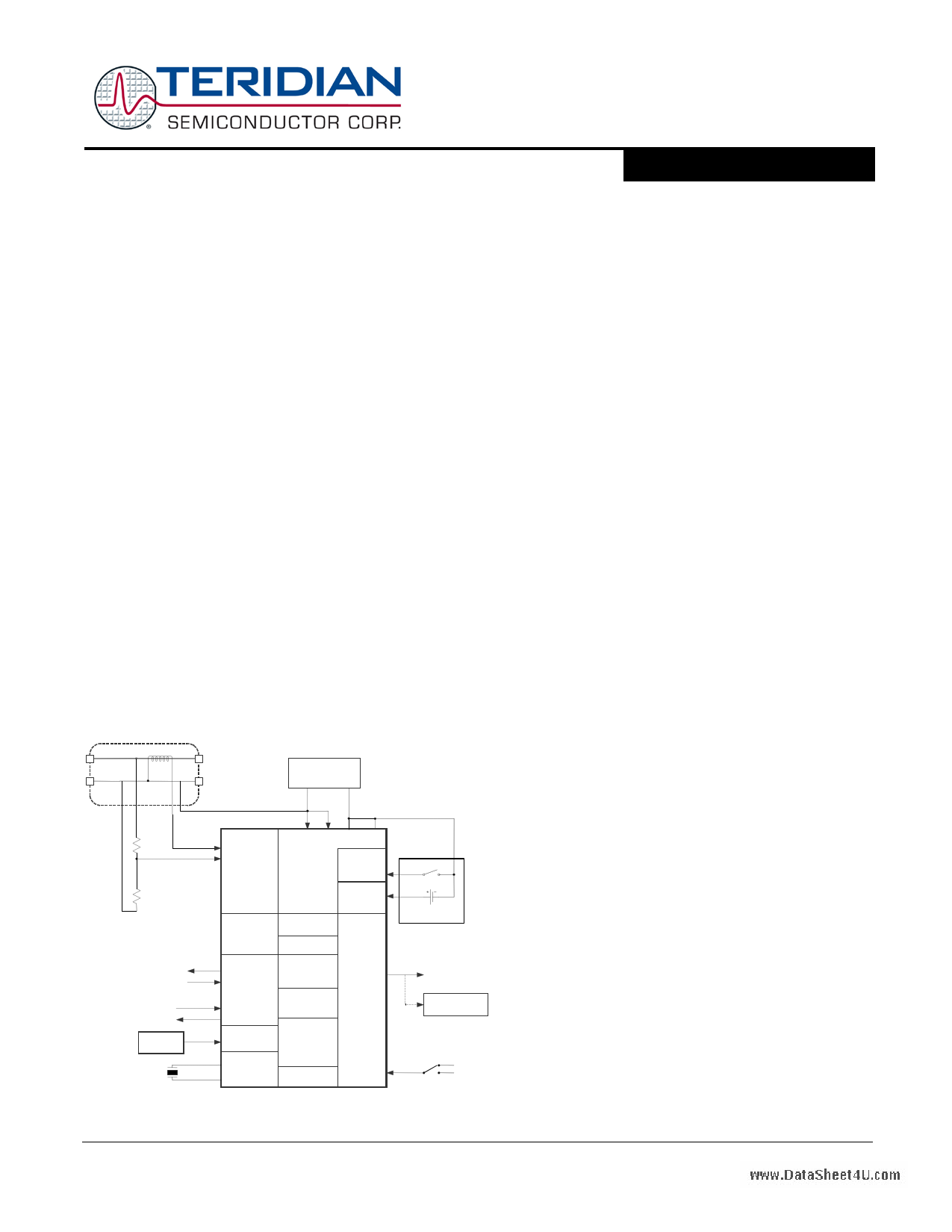
rising edge after the last mux state of its sequence, the mux will wait one additional CK32 cycle before
beginning a new frame. At the beginning of this cycle, the value of CROSS will be updated according to
the CHOP_E bits. The extra CK32 cycle allows time for the chopped VREF to settle. During this cycle,
MUXSYNC is held high. The leading edge of muxsync initiates a pass through the CE program
sequence. The beginning of the sequence is the serial readout of the four RTM words.
CHOP_E has 3 states: positive, reverse, and chop. In the positive state, CROSS is held low. In the
reverse state, CROSS is held high. In the chop state, CROSS is toggled near the end of each Mux
Frame, as described above. It is desirable that CROSS take on alternate values at the beginning of each
Mux cycle. For this reason, if chop state is selected, CROSS will not toggle at the end of the last Mux
cycle in a SUM cycle.
The internal bias voltage VBIAS (typically 1.6 V) is used by the ADC when measuring the temperature
and battery monitor signals.
1.2.5 Temperature Sensor
The 78M6612 includes an on-chip temperature sensor implemented as a bandgap reference. It is used
to determine the die temperature The MPU may request an alternate multiplexer cycle containing the
temperature sensor output by asserting MUX_ALT.
The primary use of the temperature data is to determine the magnitude of compensation required to
offset the thermal drift in the system (see Section 3.3 Temperature Compensation).
1.2.6 Battery Monitor
The battery voltage is measured by the ADC during alternative multiplexer frames if the BME (Battery
Measure Enable) bit in the I/O RAM is set. While BME is set, an on-chip 45 kΩ load resistor is applied to
the battery, and a scaled fraction of the battery voltage is applied to the ADC input. After each alternative
MUX frame, the result of the ADC conversion is available at CE DRAM address 07. BME is ignored and
assumed zero when system power is not available (V1 < VBIAS). See Section 5.4.4 Battery Monitor for
details regarding the ADC LSB size and the conversion accuracy.
1.2.7 Functional Description
The AFE functions as a data acquisition system, controlled by the MPU. The main signals (IA, VA, IB,
VB) are sampled and the ADC counts obtained are stored in CE DRAM where they can be accessed by
the CE and, if necessary, by the MPU. Alternate multiplexer cycles are initiated less frequently by the
MPU to gather access to the slow temperature and battery signals.
VREF
IA
VA
IB
VB
VBAT
MUX
VBIAS
TEMP
MUX
MUX
CTRL
EQU
MUX_ALT
CHOP_E
MUX_DIV
VREF
VREF_CAL
VREF_DIS
CROSS
CK32
VBIAS
∆Σ ADC
CONVERTER
V3P3A
-
+
ADC_E
VREF
FIR_DONE
FIR_START
4.9MHz
Figure 3: AFE Block Diagram
FIR
FIR_LEN
Rev. 1.2
11
11 Page | ||
| Páginas | Total 70 Páginas | |
| PDF Descargar | [ Datasheet 78M6612.PDF ] | |
Hoja de datos destacado
| Número de pieza | Descripción | Fabricantes |
| 78M6610+PSU | Energy Measurement Processor | Maxim Integrated |
| 78M6612 | Dual-Outlet Power and Energy Measurement IC | TERIDIAN Semiconductor |
| 78M6613 | Single-Phase AC Power Measurement IC | Teridian Semiconductor |
| 78M6618 | Octal Power and Energy Measurement IC | TERIDIAN Semiconductor |
| Número de pieza | Descripción | Fabricantes |
| SLA6805M | High Voltage 3 phase Motor Driver IC. |
Sanken |
| SDC1742 | 12- and 14-Bit Hybrid Synchro / Resolver-to-Digital Converters. |
Analog Devices |
|
DataSheet.es es una pagina web que funciona como un repositorio de manuales o hoja de datos de muchos de los productos más populares, |
| DataSheet.es | 2020 | Privacy Policy | Contacto | Buscar |