|
|
|
PDF 71M6521BE Data sheet ( Hoja de datos )
| Número de pieza | 71M6521BE | |
| Descripción | Energy Meter IC | |
| Fabricantes | TERIDIAN Semiconductor | |
| Logotipo | ||
Hay una vista previa y un enlace de descarga de 71M6521BE (archivo pdf) en la parte inferior de esta página. Total 70 Páginas | ||
|
No Preview Available !
GENERAL DESCRIPTION
The TERIDIAN 71M6521BE is a highly integrated SOC with an MPU core,
FLASH and LCD driver. TERIDIAN’s patented Single Converter Technol-
ogy™ with a 22-bit delta-sigma ADC, four analog inputs, digital temperature
compensation, precision voltage reference, battery voltage monitor, and 32-
bit computation engine (CE) supports a wide range of residential metering
applications with very few low-cost external components. A 32kHz crystal
time-base for the entire system further reduces system cost. The IC
supports 2-wire single-phase residential metering along with tamper-
detection mechanisms.
Maximum design flexibility is provided by multiple UARTs, I2C, μWire, up to
14 DIO pins and in-system programmable FLASH memory, which can be
updated with data or application code in operation.
A complete array of ICE and development tools, programming libraries and
reference designs enable rapid development and certification of AMR and
Prepay meters that comply with worldwide electricity metering standards.
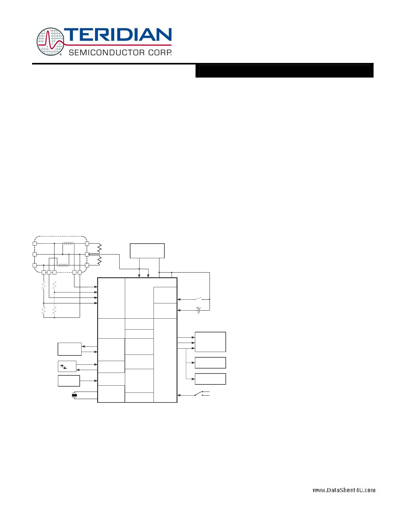
A
NEUT
B
CT/SHUNT
LOAD
LOAD
POWER SUPPLY
AMR
RX/DIO1
IR TX/DIO2
POWER
FAULT
32 kHz
CONVERTER
IA
VA
IB
VB
V3.3A
V3.3
SYS
TERIDIAN
71M6521BE
GNDA GNDD
PWR MODE
CONTROL
WAKE-UP
REGULATOR
VBAT
V2.5
VOLTAGE REF
VREF
VBIAS
SERIAL PORTS
TX
RX
SENSE
DRIVE/MOD
COMPARATOR
V1
OSC/PLL
XIN
XOUT
TEMP
SENSOR
RAM
FLASH
COMPUTE
ENGINE
MPU
TIMERS
ICE
DIO, PULSE
COM0..3
SEG0..18
SEG 24..31/
DIO 4..11
SEG 34..37/
DIO 14..17
SEG 32,33,
38
ICE_E
11/14/2007
BATTERY
3.3V LCD
888888.88
I2C or µWire
EEPROM
TEST PULSE
V3P3D
GNDD
www.DataSheet4U.com
71M6521BE
Energy Meter IC
DATA SHEET
JANUARY 2008
FEATURES
• < 0.4% Wh accuracy over 2000:1 current range
and over temperature
• Exceeds IEC62053 / ANSI C12.20 standards
• Voltage reference < 40ppm/°C
• Four sensor inputs—VDD referenced
• Low jitter Wh test output (10kHz maximum)
• Pulse count for Wh pulse output
• Tamper detection: Neutral current with CT or
shunt
• Line frequency count for time keeping
• Digital temperature compensation
• Sag detection for phase A and B
• Independent 32-bit compute engine
• 46-64Hz line frequency range with same
calibration
• Phase compensation (±7°)
• Battery monitor
• Three battery modes w/ wake-up on push-button
or timer:
Brownout mode (48µA)
LCD mode (5.7µA)
Sleep mode (2.9µA)
• Energy display on main power failure
• Wake-up with push-button
• 22-bit delta-sigma ADC
• 8-bit MPU (80515), 1 clock cycle per instruction
w/ integrated ICE for MPU debug
• Hardware watchdog timer, power fail monitor
• LCD driver (up to 140 pixels)
• Up to 14 general purpose I/O pins
• 32kHz time base
• 8KB FLASH with security
• 2KB MPU XRAM
• Two UARTs for IR and AMR
• Digital I/O pins compatible with 5V inputs
• 64-pin LQFP
• Lead Free package
V1.0
© 2005-2008 TERIDIAN Semiconductor Corporation
Page: 1 of 97
1 page 
www.DataSheet4U.com
71M6521BE
Energy Meter IC
List of Figures
DATA SHEET
JANUARY 2008
Figure 1: IC Functional Block Diagram...........................................................................................................................8
Figure 2: General Topology of a Chopped Amplifier ....................................................................................................11
Figure 3: AFE Block Diagram.......................................................................................................................................12
Figure 4: Samples from Multiplexer Cycle....................................................................................................................14
Figure 5: Accumulation Interval....................................................................................................................................15
Figure 6: Interrupt Structure .........................................................................................................................................36
Figure 7: Optical Interface ............................................................................................................................................39
Figure 8: Connecting an External Load to DIO Pins.....................................................................................................40
Figure 9: 3-Wire Interface. Write Command, HiZ=0. ....................................................................................................43
Figure 10: 3-Wire Interface. Write Command, HiZ=1 ...................................................................................................43
Figure 11: 3-Wire Interface. Read Command...............................................................................................................44
Figure 12: 3-Wire Interface. Write Command when CNT=0 .........................................................................................44
Figure 13: 3-Wire Interface. Write Command when HiZ=1 and WFR=1.......................................................................44
Figure 14: Functions defined by V1..............................................................................................................................45
Figure 15: Voltage. Current, Momentary and Accumulated Energy .............................................................................47
Figure 16: Timing Relationship between ADC MUX, Compute Engine, and Serial Transfers. .....................................48
Figure 17: RTM Output Format ....................................................................................................................................49
Figure 18: Operation Modes State Diagram.................................................................................................................50
Figure 19: Functional Blocks in BROWNOUT Mode (inactive blocks grayed out)........................................................52
Figure 20: Functional Blocks in LCD Mode (inactive blocks grayed out)......................................................................53
Figure 21: Functional Blocks in SLEEP Mode (inactive blocks grayed out) .................................................................54
Figure 22: Transition from BROWNOUT to MISSION Mode when System Power Returns .........................................55
Figure 23: Power-Up Timing with V3P3SYS and VBAT tied together ..........................................................................55
Figure 24: Power-Up Timing with VBAT only ...............................................................................................................56
Figure 25: Wake Up Timing..........................................................................................................................................57
Figure 26: MPU/CE Data Flow .....................................................................................................................................58
Figure 27: MPU/CE Communication ............................................................................................................................58
Figure 28: Resistive Voltage Divider (Left), Current Transformer (Right) .....................................................................60
Figure 29: Resistive Shunt ...........................................................................................................................................60
Figure 30: Connecting LCDs ........................................................................................................................................61
Figure 31: I2C EEPROM Connection............................................................................................................................63
Figure 32: Three-Wire EEPROM Connection...............................................................................................................63
Figure 33: Connections for the RX Pin .........................................................................................................................64
Figure 34: Connection for Optical Components ...........................................................................................................65
Figure 35: Voltage Divider for V1 .................................................................................................................................65
Figure 36: External Components for the RESET Pin: Push-Button (Left), EMI Circuit (Right) .....................................66
Figure 37: External Components for the Emulator Interface ........................................................................................66
Figure 38: Wh Accuracy, 0.1A to 200A at 240V/50Hz and Room Temperature...........................................................91
Figure 39: Meter Accuracy over Harmonics at 240V, 30A............................................................................................91
Figure 40: Typical Meter Accuracy over Temperature Relative to 25°C.......................................................................92
V1.0
© 2005-2008 TERIDIAN Semiconductor Corporation
Page: 5 of 97
5 Page 
Vinp
Vinn
A
B
A
B
CROSS
+
G
-
www.DataSheet4U.com
71M6521BE
Energy Meter IC
DATA SHEET
JANUARY 2008
A Voutp
B
A Voutn
B
Figure 2: General Topology of a Chopped Amplifier
It is assumed that an offset voltage Voff appears at the positive amplifier input. With all switches, as controlled by CROSS in
the “A” position, the output voltage is:
Voutp – Voutn = G (Vinp + Voff – Vinn) = G (Vinp – Vinn) + G Voff
With all switches set to the “B” position by applying the inverted CROSS signal, the output voltage is:
Voutn – Voutp = G (Vinn – Vinp + Voff) = G (Vinn – Vinp) + G Voff, or
Voutp – Voutn = G (Vinp – Vinn) - G Voff
Thus, when CROSS is toggled, e.g. after each multiplexer cycle, the offset will alternately appear on the output as positive and
negative, which results in the offset effectively being eliminated, regardless of its polarity or magnitude.
When CROSS is high, the hookup of the amplifier input devices is reversed. This preserves the overall polarity of that
amplifier gain, it inverts its input offset. By alternately reversing the connection, the amplifier’s offset is averaged to zero. This
removes the most significant long-term drift mechanism in the voltage reference. The CHOP_E bits control the behavior of
CROSS. The CROSS signal will reverse the amplifier connection in the voltage reference in order to negate the effects of its
offset. On the first CK32 rising edge after the last mux state of its sequence, the mux will wait one additional CK32 cycle
before beginning a new frame. At the beginning of this cycle, the value of CROSS will be updated according to the CHOP_E
bits. The extra CK32 cycle allows time for the chopped VREF to settle. During this cycle, MUXSYNC is held high. The
leading edge of muxsync initiates a pass through the CE program sequence. The beginning of the sequence is the serial
readout of the 4 RTM words.
CHOP_E has 3 states: positive, reverse, and chop. In the ‘positive’ state, CROSS is held low. In the ‘reverse’ state, CROSS is
held high. In the ‘chop’ state, CROSS is toggled near the end of each Mux Frame, as described above. It is desirable that
CROSS take on alternate values at the beginning of each Mux cycle. For this reason, if ‘chop’ state is selected, CROSS will
not toggle at the end of the last Mux cycle in a SUM cycle.
The internal bias voltage VBIAS (typically 1.6V) is used by the ADC when measuring the temperature and battery monitor
signals.
Temperature Sensor
The 71M6521BE includes an on-chip temperature sensor implemented as a bandgap reference. It is used to determine the die
temperature The MPU may request an alternate multiplexer cycle containing the temperature sensor output by asserting
MUX_ALT.
The primary use of the temperature data is to determine the magnitude of compensation required to offset the thermal drift in
the system (see section titled “Temperature Compensation”).
V1.0
© 2005-2008 TERIDIAN Semiconductor Corporation
Page: 11 of 97
11 Page | ||
| Páginas | Total 70 Páginas | |
| PDF Descargar | [ Datasheet 71M6521BE.PDF ] | |
Hoja de datos destacado
| Número de pieza | Descripción | Fabricantes |
| 71M6521BE | Energy Meter IC | TERIDIAN Semiconductor |
| Número de pieza | Descripción | Fabricantes |
| SLA6805M | High Voltage 3 phase Motor Driver IC. |
Sanken |
| SDC1742 | 12- and 14-Bit Hybrid Synchro / Resolver-to-Digital Converters. |
Analog Devices |
|
DataSheet.es es una pagina web que funciona como un repositorio de manuales o hoja de datos de muchos de los productos más populares, |
| DataSheet.es | 2020 | Privacy Policy | Contacto | Buscar |