|
|
|
PDF ADF4158 Data sheet ( Hoja de datos )
| Número de pieza | ADF4158 | |
| Descripción | Direct Modulation/Waveform Generating 6.1 GHz Fractional-N Frequency Synthesizer | |
| Fabricantes | Analog Devices | |
| Logotipo | ||
Hay una vista previa y un enlace de descarga de ADF4158 (archivo pdf) en la parte inferior de esta página. Total 30 Páginas | ||
|
No Preview Available !
Data Sheet
Direct Modulation/Waveform Generating,
6.1 GHz Fractional-N Frequency Synthesizer
ADF4158
FEATURES
GENERAL DESCRIPTION
Radio frequency (RF) bandwidth to 6.1 GHz
25-bit fixed modulus allows subhertz frequency resolution
Frequency and phase modulation capability
Sawtooth and triangular waveforms in the frequency domain
Parabolic ramp
Ramp superimposed with FSK
Ramp with 2 different sweep rates
Ramp delay
Ramp frequency readback
Ramp interruption
2.7 V to 3.3 V power supply
Separate VP allows extended tuning voltage
Programmable charge pump currents
3-wire serial interface
Digital lock detect
Power-down mode
Cycle slip reduction for faster lock times
Switched bandwidth fast-lock mode
Qualified for automotive applications
APPLICATIONS
The ADF4158 is a 6.1 GHz fractional-N frequency synthesizer
with direct modulation and waveform generation capability. It
contains a 25-bit fixed modulus, allowing subhertz resolution at
6.1 GHz. It consists of a low noise digital phase frequency
detector (PFD), a precision charge pump, and a programmable
reference divider. There is a sigma-delta (Σ-Δ) based fractional
interpolator to allow programmable fractional-N division. The
INT and FRAC registers define an overall N-divider as N = INT +
(FRAC/225).
The ADF4158 can be used to implement frequency shift keying
(FSK) and phase shift keying (PSK) modulation. There are also
a number of frequency sweep modes available that generate
various waveforms in the frequency domain, for example,
sawtooth and triangular waveforms. The ADF4158 features
cycle slip reduction circuitry, which leads to faster lock times,
without the need for modifications to the loop filter.
Control of all on-chip registers is via a simple 3-wire interface.
The device operates with a power supply ranging from 2.7 V to
3.3 V and can be powered down when not in use.
Frequency modulated continuous wave (FMCW) radar
Communications test equipment
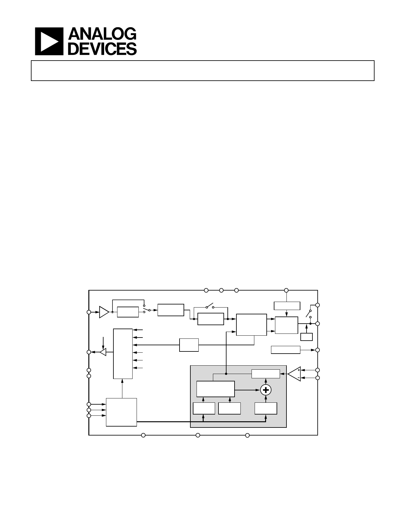
FUNCTIONAL BLOCK DIAGRAM
AVDD DVDD VP
RSET
ADF4158
REFIN
MUXOUT
CE
TXDATA
×2
DOUBLER
5-BIT
R-COUNTER
÷2
DIVIDER
HIGH-Z
OUTPUT
MUX
VDD
DGND
VDD
RDIV
NDIV
LOCK
DETECT
+ PHASE
FREQUENCY
DETECTOR
–
REFERENCE
CHARGE
PUMP
CSR
FLO SWITCH
N-COUNTER
THIRD-ORDER
FRACTIONAL
INTERPOLATOR
SW2
CP
SW1
RFINA
RFINB
CLK
DATA
LE
32-BIT
DATA
REGISTER
FRACTION MODULUS
REG
225
INTEGER
REG
AGND
DGND
Figure 1.
CPGND
Rev. G
Document Feedback
Information furnished by Analog Devices is believed to be accurate and reliable. However, no
responsibilityisassumedbyAnalogDevices for itsuse,nor foranyinfringementsofpatentsor other
rights of third parties that may result from its use. Specifications subject to change without notice. No
license is granted by implication or otherwise under any patent or patent rights of Analog Devices.
Trademarksandregisteredtrademarksarethepropertyoftheirrespectiveowners.
One Technology Way, P.O. Box 9106, Norwood, MA 02062-9106, U.S.A.
Tel: 781.329.4700 ©2010–2014 Analog Devices, Inc. All rights reserved.
Technical Support
www.analog.com
1 page 
Data Sheet
ADF4158
Parameter
NOISE CHARACTERISTICS
Normalized Phase Noise Floor
(PNSYNTH)4
Normalized 1/f Noise (PN1_f)5
Phase Noise Performance6
5805 MHz Output7
C Version1
Min Typ Max Unit
Test Conditions/Comments
−216
−110
−93
dBc/Hz
dBc/Hz
dBc/Hz
PLL loop bandwidth = 500 kHz;
measured at 100 kHz offset
100 kHz offset; normalized to 1 GHz
At VCO output
At 5 kHz offset, 32 MHz PFD frequency
1 Operating temperature for C version: −40°C to +125°C.
2 AC coupling ensures AVDD/2 bias.
3 Guaranteed by design. Sample tested to ensure compliance.
4 The synthesizer phase noise floor is estimated by measuring the in-band phase noise at the output of the VCO and subtracting 20 log(N) (where N is the N divider
value) and 10 log(fPFD). PNSYNTH = PNTOT − 10 log(fPFD) − 20 log(N).
5 The PLL phase noise is composed of 1/f (flicker) noise plus the normalized PLL noise floor. The formula for calculating the 1/f noise contribution at an RF frequency, fRF,
and at a frequency offset f is given by PN = PN1_f + 10 log(10 kHz/f) + 20 log(fRF/1 GHz). Both the normalized phase noise floor and flicker noise are modeled in ADIsimPLL™.
6 The phase noise is measured with the EVAL-ADF4158EB1Z and the Agilent E5052A phase noise system.
7 fREFIN = 128 MHz; fPFD = 32 MHz; offset frequency = 5 kHz; RFOUT = 5805 MHz; INT = 181; FRAC = 13631488; loop bandwidth = 100 kHz.
TIMING SPECIFICATIONS
AVDD = DVDD = SDVDD = 2.7 V to 3.3 V; VP = AVDD to 5.5 V; AGND = DGND = SDGND = 0 V; TA = TMIN to TMAX, dBm referred to 50 Ω,
unless otherwise noted.
Table 2. Write Timing
Parameter
Limit at TMIN to TMAX (C Version)
t1 20
t2 10
t3 10
t4 25
t5 25
t6 10
t7 20
Unit
ns min
ns min
ns min
ns min
ns min
ns min
ns min
Test Conditions/Comments
LE setup time
DATA to CLK setup time
DATA to CLK hold time
CLK high duration
CLK low duration
CLK to LE setup time
LE pulse width
Write Timing Diagram
CLK
DATA
DB31 (MSB)
LE
t1
LE
t4 t5
t2 t3
DB30
DB2
(CONTROL BIT C3)
DB1
(CONTROL BIT C2)
Figure 2. Write Timing Diagram
DB0 (LSB)
(CONTROL BIT C1)
t7
t6
Rev. G | Page 5 of 36
5 Page 
Data Sheet
CIRCUIT DESCRIPTION
REFERENCE INPUT SECTION
The reference input stage is shown in Figure 16. SW1 and SW2
are normally closed switches. SW3 is normally open. When
power-down is initiated, SW3 is closed and SW1 and SW2 are
opened. This ensures that there is no loading of the REFIN pin
on power-down.
POWER-DOWN
CONTROL
NC 100kΩ
REFIN NC
SW2
SW1
SW3
NO
TO R-COUNTER
BUFFER
Figure 16. Reference Input Stage
RF INPUT STAGE
The RF input stage is shown in Figure 17. It is followed by a
2-stage limiting amplifier to generate the current-mode logic
(CML) clock levels needed for the prescaler.
BIAS
GENERATOR
1.6V
2kΩ 2kΩ
AVDD
RFINA
RFINB
Figure 17. RF Input Stage
AGND
RF INT DIVIDER
The RF INT CMOS counter allows a division ratio in the PLL
feedback counter. Division ratios from 23 to 4095 are allowed.
ADF4158
25-BIT FIXED MODULUS
The ADF4158 has a 25-bit fixed modulus. This allows output
frequencies to be spaced with a resolution of
fRES = fPFD/225
(1)
where fPFD is the frequency of the phase frequency detector
(PFD). For example, with a PFD frequency of 10 MHz,
frequency steps of 0.298 Hz are possible. Due to the architecture
of the Σ-Δ modulator, there is a fixed + (fPFD/226) offset on the
VCO output. To remove this offset, see the Σ-Δ Modulator
Mode section.
INT, FRAC, AND R RELATIONSHIP
The INT and FRAC values, in conjunction with the R-counter,
make it possible to generate output frequencies that are spaced
by fractions of the phase frequency detector (PFD). The RF VCO
frequency (RFOUT) equation is
RFOUT = fPFD × (INT + (FRAC/225))
(2)
where:
RFOUT is the output frequency of external voltage controlled
oscillator (VCO).
INT is the preset divide ratio of binary 12-bit counter (23 to 4095).
FRAC is the numerator of the fractional division (0 to 225 − 1).
fPFD = REFIN × [(1 + D)/(R × (1 + T))]
(3)
where:
REFIN is the reference input frequency.
D is the REFIN doubler bit (0 or 1).
R is the preset divide ratio of the binary, 5-bit, programmable
reference counter (1 to 32).
T is the REFIN divide-by-2 bit (0 or 1).
RF N-DIVIDER
FROM RF
INPUT STAGE
N-COUNTER
N = INT + FRAC/MOD
TO PFD
THIRD-ORDER
FRACTIONAL
INTERPOLATOR
INT
REG
MOD
REG
FRAC
VALUE
Figure 18. RF N-Divider
R-COUNTER
The 5-bit R-counter allows the input reference frequency (REFIN)
to be divided down to produce the reference clock to the PFD.
Division ratios from 1 to 32 are allowed.
Rev. G | Page 11 of 36
11 Page | ||
| Páginas | Total 30 Páginas | |
| PDF Descargar | [ Datasheet ADF4158.PDF ] | |
Hoja de datos destacado
| Número de pieza | Descripción | Fabricantes |
| ADF4150 | Fractional-N/Integer-N PLL Synthesizer | Analog Devices |
| ADF4150HV | Fractional-N/Integer-N PLL Synthesizer | Analog Devices |
| ADF4151 | Fractional-N/Integer-N PLL Synthesizer | Analog Devices |
| ADF4152HV | Fractional-N/ Integer N PLL Synthesizer | Analog Devices |
| Número de pieza | Descripción | Fabricantes |
| SLA6805M | High Voltage 3 phase Motor Driver IC. |
Sanken |
| SDC1742 | 12- and 14-Bit Hybrid Synchro / Resolver-to-Digital Converters. |
Analog Devices |
|
DataSheet.es es una pagina web que funciona como un repositorio de manuales o hoja de datos de muchos de los productos más populares, |
| DataSheet.es | 2020 | Privacy Policy | Contacto | Buscar |