|
|
|
PDF ICS674-01 Data sheet ( Hoja de datos )
| Número de pieza | ICS674-01 | |
| Descripción | User Configurable Divider | |
| Fabricantes | Integrated Circuit Systems | |
| Logotipo | ||
Hay una vista previa y un enlace de descarga de ICS674-01 (archivo pdf) en la parte inferior de esta página. Total 6 Páginas | ||
|
No Preview Available !
PRELIMINARY INFORMATION
ICS674-01
User Configurable Divider
Description
Features
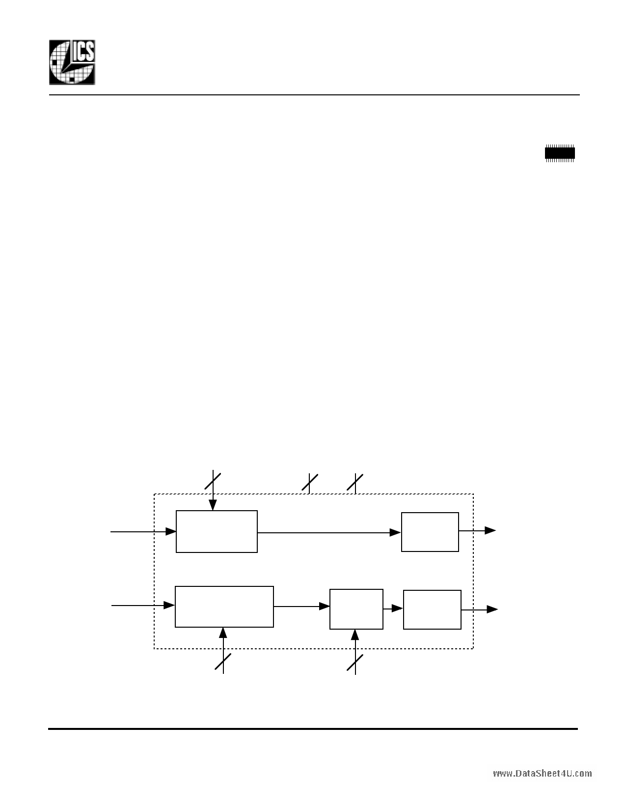
The ICS674-01 consists of 2 separate
configurable dividers. The A Divider is a 7 bit
divider and can divide by 3 to 129. The
B Divider consists of a 9 bit divider followed by a
post divider. The 9 bit divider can divide by 12
to 519. The post divider has eight settings of
1, 2, 4, 5, 6, 7, 8 and 10 giving a maximum total
wwwd.DiavtiadSeheoef t54U1.9co0m. The A and B Dividers can be
cascaded to give a maximum divide of 669510.
The ICS674-01 supports the ICS673 PLL
Building Block and enables the user to build a full
custom PLL synthesizer.
• Packaged as 28 pin SSOP (150 mil body)
• Supports ICS673 PLL Building Block
• User determines the divide by setting input pins
• Pull-ups on all select inputs
• Includes one 7-bit Divider for OUTA
• Includes one 9-bit Divider and one selectable
Post Divider for OUTB
• Operating voltages of 3.3 V or 5.0 V
• Industrial temperature range available
• 25mA drive capability at TTL levels
• Advanced, low power CMOS process
Block Diagram
A6:A0
7
INA
Divider A
(7-Bit)
VDD GND
23
Output
Buffer
OUTA
INB
Divider B
(9-Bit)
Post
Divider
Output
Buffer
OUTB
9
B8:B0
3
S2:S0
MDS 674-01 A
1
Revision 033199
Printed 11/15/00
Integrated Circuit Systems • 525 Race Street • San Jose • CA • 95126 •(408)295-9800tel•(408)295-9818fax
1 page 
PRELIMINARY INFORMATION
ICS674-01
User Configurable Divider
Parameter
Conditions
Minimum Typical
ABSOLUTE MAXIMUM RATINGS (stresses be ond these can permanentl damage the device)
Supply Voltage, VDD
Referenced to GND
Inputs
Referenced to GND
-0.5
Clock Output
Referenced to GND
-0.5
Ambient Operating Temperature
0
Ambient Operating Temperature
I version
-40
Soldering Temperature
Max of 10 seconds
wwwS.DtoartaagSeheTeetm4Up.ecroamture
DC CHARACTERISTICS (VDD = 5.0V unless otherwise noted)
-65
Operating Voltage, VDD
3
Input High Voltage, VIH
All A, B, and S pins
2
Input Low Voltage, VIL
All A, B, and S pins
Input High Voltage, VIH, INA and INB only
(VDD/2)+1 VDD/2
Input Low Voltage, VIL, INA and INB only
VDD/2
Output High Voltage, VOH
IOH=-25mA
2.4
Output Low Voltage, VOL
IOL=25mA
IDD, Op. Supply Cur., DivA=DivB=20 at 3.3 V No Load, fin=100 MHz
3
IDD, Op. Supply Cur., DivA=DivB=20 at 5 V
No Load, fin=100 MHz
5
Short Circuit Current, outputs
±70
On-Chip Pull-up Resistor
A, B, S select pins
270
Input Capacitance
A, B, S select pins
5
AC CHARACTERISTICS (VDD = 5.0V unless otherwise noted)
Input Frequency, Divider A
at 3.3 V
0
Input Frequency, Divider B
at 3.3 V
0
Input Frequency, Divider A
at 5 V
0
Input Frequency, Divider B
at 5 V
0
Input Frequency, Divider A (Industrial temperature) at 3.3 V at 85 °C
0
Input Frequency, Divider B (Industrial temperature) at 3.3 V at 85 °C
0
Input Frequency, Divider A (Industrial temperature) at 5 V at 85 °C
0
Input Frequency, Divider B (Industrial temperature) at 5 V at 85 °C
0
Output Clock Rise Time
0.8 to 2.0V
1
Output Clock Fall Time
2.0 to 0.8V
1
OUTB Clock Duty Cycle (see note)
at VDD/2
45 49 to 51
OUTB Clock Duty Cycle, odd post dividers
at VDD/2, except PD=1
40
OUTA Clock Duty Cycle (see note)
at VDD/2
20
Maximum Units
7
VDD+0.5
VDD+0.5
70
85
260
150
V
V
V
°C
°C
°C
°C
5.5
0.8
(VDD/2)-1
0.4
V
V
V
V
V
V
V
mA
mA
mA
kΩ
pF
135 M H z
180 M H z
200 M H z
235 M H z
125 M H z
170 M H z
190 M H z
220 M H z
ns
ns
55 %
60 %
98.5 %
Note:
The duty cycle of OUTA is dependent on the selected divide. This is because OUTA goes low for 2 input
clock cycles on INA. So, for example, if a divide of 20 is selected, the duty cycle will be 90%.
Similarly, if PD=1 is selected for OUTB, the duty cycle will be dependent on the selected divide. In this
case OUTB goes high for approximately 8 input clock cycles on INB.
MDS 674-01 A
5
Revision 033199
Printed 11/15/00
Integrated Circuit Systems • 525 Race Street • San Jose • CA • 95126 •(408)295-9800tel•(408)295-9818fax
5 Page | ||
| Páginas | Total 6 Páginas | |
| PDF Descargar | [ Datasheet ICS674-01.PDF ] | |
Hoja de datos destacado
| Número de pieza | Descripción | Fabricantes |
| ICS674-01 | User Configurable Divider | Integrated Circuit Systems |
| Número de pieza | Descripción | Fabricantes |
| SLA6805M | High Voltage 3 phase Motor Driver IC. |
Sanken |
| SDC1742 | 12- and 14-Bit Hybrid Synchro / Resolver-to-Digital Converters. |
Analog Devices |
|
DataSheet.es es una pagina web que funciona como un repositorio de manuales o hoja de datos de muchos de los productos más populares, |
| DataSheet.es | 2020 | Privacy Policy | Contacto | Buscar |