|
|
|
PDF NJG1122PB4 Data sheet ( Hoja de datos )
| Número de pieza | NJG1122PB4 | |
| Descripción | Dual LNA | |
| Fabricantes | JRC | |
| Logotipo | ||
Hay una vista previa y un enlace de descarga de NJG1122PB4 (archivo pdf) en la parte inferior de esta página. Total 28 Páginas | ||
|
No Preview Available !
www.DataSheet4U.com
NJG1122PB4
W-CDMA Dual LNA GaAs MMIC
QGENERAL DESCRIPTION
QPACKAGE OUTLINE
The NJG1122PB4 is a Dual band LNA IC designed for W-CDMA
cellular phone of 2.1GHz and 800MHz band.
This IC has a LNA pass-through function to select high gain mode
or low gain mode.
An ultra small and ultra thin package of FFP12–B4 is adopted.
NJG1122PB4
QFEATURES
OLow voltage operation
OLow CTL voltage operation
OLow current consumption
+2.7V
+1.85V
2.4mA typ. @2.1GHz band (High Gain Mode)
2.0mA typ. @800MHz band (High Gain Mode)
OSmall package
4uA typ. @800MHz / 2.1GHz band (Low Gain Mode)
FFP12-B4 (Package size: 2.0 x 2.0 x 0.65mm typ)
[High gain mode]
OHigh gain
OLow noise figure
OHigh Input IP3
[Low gain mode]
OGain
OLow noise figure
OHigh Input IP3
14.5dB typ. @fRF =2140MHz16.0dB typ. @fRF =885MHz
1.7dB typ. @fRF=2140MHz
1.45dB typ. @fRF =885MHz
-3.5dBm typ. @ fRF=2140.0+2140.1MHz, Pin=-36dBm
-3.5dBm typ. @fRF=885.0+885.1MHz, Pin=-36dBm
-4.0dB typ. @fRF=2140MHz
-4.5dB typ. @fRF=885MHz
4.0dB typ. @fRF=2140MHz
4.5dB typ. @fRF=885MHz
+2.5dBm typ. @fRF=2140.0+2140.1MHz, Pin=-20dBm
+2.0dBm typ. @fRF=885.0+885.1MHz, Pin=-20dBm
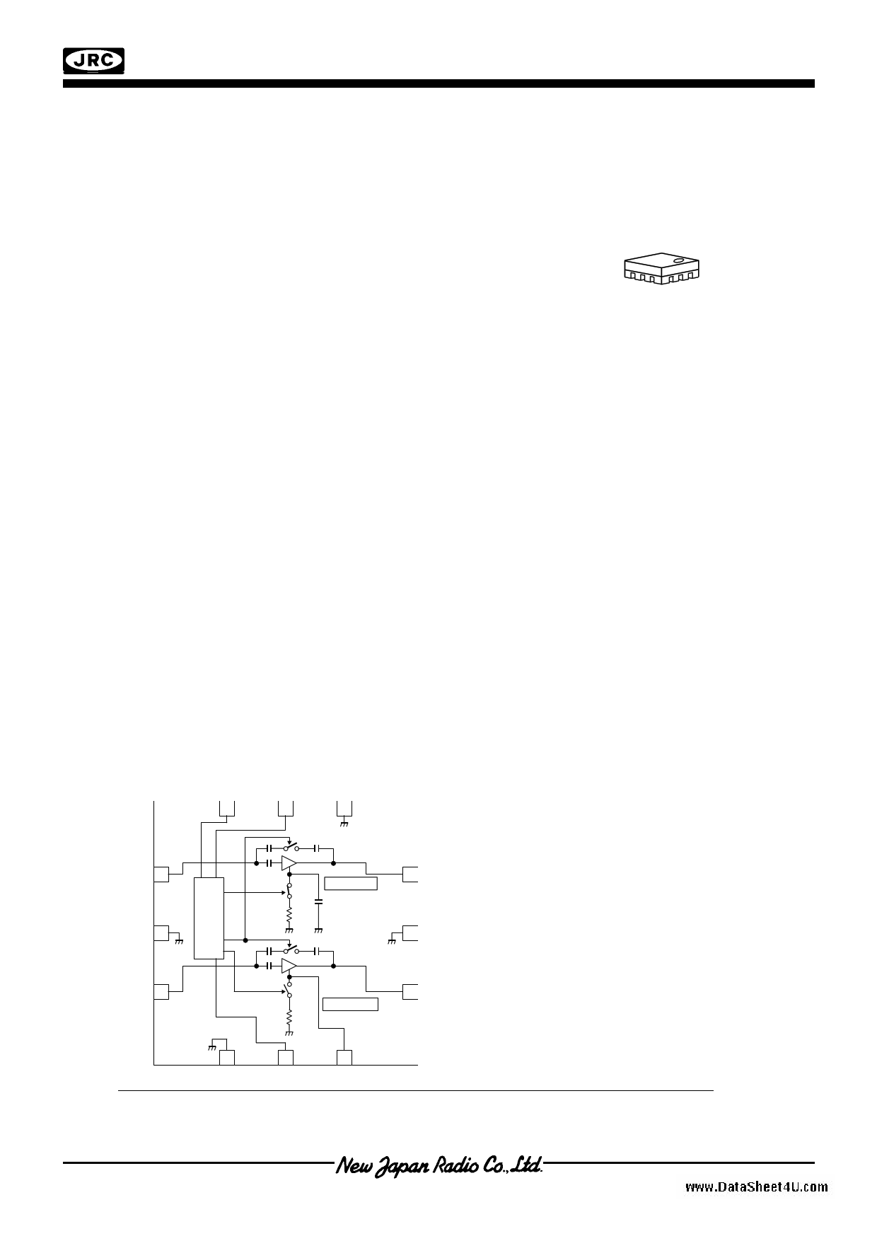
QPIN CONFIGURATION
(Top View)
VINV 9
VCTL1 8
GND 7
RFIN2
10
GND
11
RFIN1
12
2.1GHz Band
RFOUT2
6
GND
5
800MHz Band
RFOUT1
4
Pin Connection
1. GND
2. VCTL2
3. EXTCAP
4. RFOUT1 (800MHz band)
5. GND
6. RFOUT2 (2.1GHz band)
7. GND
8. VCTL1
9. VINV
10. RFIN2 (2.1GHz band)
11. GND
12. RFIN1 (800MHz band)
GND 1
VCTL2 2 EXTCAP 3
Note: Specifications and description listed in this catalog are subject to change without prior notice.
Ver.2005-08-29
-1-
1 page 
www.DataSheet4U.com
QTERMINAL INFORMATION
NJG1122PB4
No. SYMBOL
DESCRIPTION
1 GND Ground terminal. (0V)
2
VCTL2
Control voltage supply terminal. The high level voltage of this terminal selects High Gain
Mode. The low level voltage of this terminal selects Low Gain Mode.
3 EXTCAP An external bypass capacitor is required. (Please refer to TEST CIRCUIT.)
4
RFOUT1
Output terminal of 800MHz band. This terminal is also the power supply terminal of the
LNA, please use inductor (L3) to connect power supply.
5 GND Ground terminal. (0V)
6
RFOUT2
Output terminal of 2.1GHz band. This terminal is also the power supply terminal of the
LNA, please use inductor (L7) to connect power supply.
7 GND Ground terminal. (0V)
8
VCTL1
Control voltage supply terminal. The high level voltage of this terminal selects
800MHz.band. The low level voltage of this terminal selects 2.1GHz band.
9 VINV Inverter voltage supplies terminal.
10
RFIN2
RF input terminal of 2.1GHz band. The RF signal is input through external matching circuit
connected to this terminal. The DC blocking capacitor is not required.
11 GND Ground terminal. (0V)
12
RFIN1
RF input terminal of 800MHz band. The RF signal is input through external matching
circuit connected to this terminal. The DC blocking capacitor is not required.
CAUTION
1) Ground terminal (No.1, 5, 7, 11) should be connected to the ground plane as low inductance as possible.
-5-
5 Page 
www.DataSheet4U.com
QELECTRICAL CHARACTERISTICS 6 (2.1GHz band Low Gain Mode)
NJG1122PB4
Pout vs. Pin
(f=2140MHz, VDD=VINV=2.7V, VCTL1=0V, VCTL2=0V)
10
0
-10
Pout
-20
-30
-40 P-1dB(IN)=+11.4dBm
-50
-40 -30 -20 -10
0
Pin (dBm)
10 20
Gain vs. Pin
(f=2140MHz, VDD=VINV=2.7V, VCTL1=0V, VCTL2=0V)
0
-2
-4 Gain
-6
-8
-10 P-1dB(IN)=+11.4dBm
-12
-40 -30 -20 -10
0
Pin (dBm)
10 20
NF vs. frequency
(VDD=VINV=2.7V, VCTL1=0V, VCTL2=0V)
9
8
7
6
NF
5
4
3
2
1
2 2.05 2.1 2.15 2.2 2.25 2.3
frequency (GHz)
Pout, IM3 vs. Pin
(f=2140+2140.1MHz, VDD=VINV=2.7V, VCTL1=0V, VCTL2=0V)
20
0
-20 Pout
-40
-60
IM3
-80 IIP3=+5.3dBm
-100
-40 -30 -20 -10
0
10
Pin (dBm)
OIP3, IIP3 vs. frequency
(df=100kHz, Pin=-36dBm, VDD=VINV=2.7V, VCTL1=0V, VCTL2=0V)
4 16
2
0 OIP3
14
12
-2 10
-4 8
-6 IIP3 6
-8 4
-10
2.1
2.12 2.14 2.16 2.18
frequency (GHz)
2
2.2
P-1dB(IN) vs. frequency
(VDD=VINV=2.7V, VCTL1=0V, VCTL2=0V)
18
16
14
P-1dB(IN)
12
10
8
6
4
2
2.1 2.12 2.14 2.16 2.18
frequency (GHz)
2.2
- 11 -
11 Page | ||
| Páginas | Total 28 Páginas | |
| PDF Descargar | [ Datasheet NJG1122PB4.PDF ] | |
Hoja de datos destacado
| Número de pieza | Descripción | Fabricantes |
| NJG1122PB4 | Dual LNA | JRC |
| Número de pieza | Descripción | Fabricantes |
| SLA6805M | High Voltage 3 phase Motor Driver IC. |
Sanken |
| SDC1742 | 12- and 14-Bit Hybrid Synchro / Resolver-to-Digital Converters. |
Analog Devices |
|
DataSheet.es es una pagina web que funciona como un repositorio de manuales o hoja de datos de muchos de los productos más populares, |
| DataSheet.es | 2020 | Privacy Policy | Contacto | Buscar |