|
|
|
PDF X9251 Data sheet ( Hoja de datos )
| Número de pieza | X9251 | |
| Descripción | Quad Digitally-Controlled Potentiometer | |
| Fabricantes | Intersil Corporation | |
| Logotipo | ||
Hay una vista previa y un enlace de descarga de X9251 (archivo pdf) en la parte inferior de esta página. Total 21 Páginas | ||
|
No Preview Available !
DATASHEET
Single Supply/Low Power/256-Tap/SPI Bus, Quad
Digitally-Controlled (XDCP™) Potentiometer
X9251
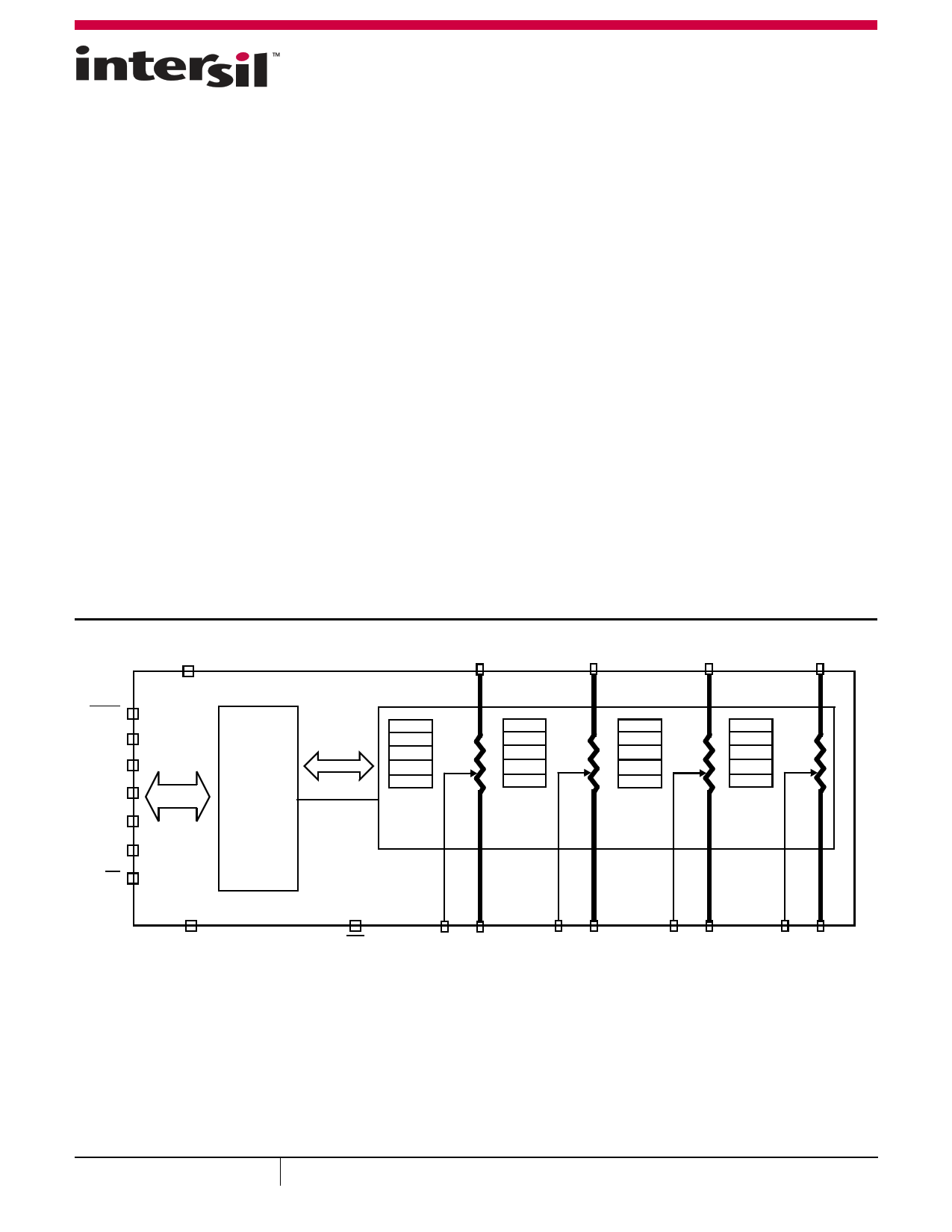
The X9251 integrates four digitally controlled potentiometers
(XDCP) on a monolithic CMOS integrated circuit.
The digitally controlled potentiometers are implemented with
a combination of resistor elements and CMOS switches. The
position of the wipers are controlled by the user through the
SPI bus interface. Each potentiometer has associated with it a
volatile Wiper Counter Register (WCR) and four nonvolatile
Data Registers that can be directly written to and read by the
user. The content of the WCR controls the position of the wiper.
At power-up, the device recalls the content of the default Data
Registers of each DCP (DR00, DR10, DR20, and DR30) to the
corresponding WCR.
The XDCP can be used as a three terminal potentiometer or as
a two terminal variable resistor in a wide variety of
applications including control, parameter adjustments, and
signal processing.
Features
• Four potentiometers in one package
• 256 resistor taps–0.4% resolution
• SPI serial interface for write, read, and transfer operations of
the potentiometer
• Wiper resistance: 100Ω typical at VCC = 5V
• 4 Nonvolatile data registers for each potentiometer
• Nonvolatile storage of multiple wiper positions
• Standby current <5µA max
• VCC: 2.7V to 5.5V operation
• 50kΩ version of total resistance
• 100 year data retention
• Single supply version of X9250
• Endurance: 100,000 data changes per bit per register
• 24 Ld SOIC, 24 Ld TSSOP
• Low power CMOS
• Pb-free (RoHS compliant)
VCC
HOLD
A1
A0
SO
SI
SCK
CS
SPI
Interface
POWER UP,
INTERFACE
CONTROL
AND
STATUS
VSS
RH0
RH1
RH2
RH3
WCR0
DR00
DR01
DR02
DR03
DCP0
WCR1
DR10
DR11
DR12
DR13
DCP1
WCR2
DR20
DR21
DR22
DR23
DCP2
WCR3
DR30
DR31
DR32
DR33
DCP3
WP
RW0 RL0
RW1 RL1
FIGURE 1. FUNCTIONAL DIAGRAM
RW2 RL2
RW3 RL3
December 3, 2014
FN8166.6
1
CAUTION: These devices are sensitive to electrostatic discharge; follow proper IC Handling Procedures.
1-888-INTERSIL or 1-888-468-3774 | Copyright Intersil Americas LLC 2005-2007, 2014. All Rights Reserved
Intersil (and design) and XDCP are trademarks owned by Intersil Corporation or one of its subsidiaries.
All other trademarks mentioned are the property of their respective owners.
1 page 
X9251
One of Four Potentiometers
#: 0, 1, 2, or 3
SERIAL DATA PATH
FROM INTERFACE
CIRCUITRY
DR#0
DR#1
SERIAL
BUS
INPUT
RH
8
DR#2
DR#3
8 PARALLEL
BUS
INPUT
WIPER
COUNTER
---
DECODE
DCP
CORE
COUNTER
REGISTER
(WCR#)
RW
IF WCR = 00[H] then RW is closest to RL
IF WCR = FF[H] then RW is closest to RH
UP/DN
MODIFIED SCK
INC/DEC
LOGIC
UP/DN
CLK
FIGURE 2. DETAILED POTENTIOMETER BLOCK DIAGRAM
RL
Power-Up and Down Recommendations
There are no restrictions on the power-up or power-down
conditions of VCC and the voltages applied to the potentiometer
pins provided that VCC is always more positive than or equal to
VH, VL, and VW (i.e., VCC VH, VL, VW). The VCC ramp rate
specification is always in effect.
Wiper Counter Register (WCR)
The X9251 contains four Wiper Counter Registers, one for each
potentiometer. The Wiper Counter Register can be envisioned as
a 8-bit parallel and serial load counter with its outputs decoded
to select one of 256 wiper positions along its resistor array. The
contents of the WCR can be altered in four ways: it may be
written directly by the host via the Write Wiper Counter Register
instruction (serial load); it may be written indirectly by
transferring the contents of one of four associated data registers
via the XFR Data Register instruction (parallel load); it can be
modified one step at a time by the Increment/Decrement
instruction (see “Instruction Format” on page 10 for more
details). Finally, it is loaded with the contents of its Data Register
zero (DR#0) upon power-up (see Figure 2).
The wiper counter register is a volatile register; that is, its
contents are lost when the X9251 is powered down. Although the
register is automatically loaded with the value in DR#0 upon
power-up, this may be different from the value present at
power-down. Power-up guidelines are recommended to ensure
proper loadings of the DR#0 value into the WCR#.
Data Registers (DR)
Each of the four DCPs has four 8-bit nonvolatile Data Registers.
These can be read or written directly by the host. Data can also
be transferred between any of the four Data Registers and the
associated Wiper Counter Register. All operations changing data
in one of the Data Registers is a nonvolatile operation and takes
a maximum of 10ms.
If the application does not require storage of multiple settings for
the potentiometer, the Data Registers can be used as regular
memory locations for system parameters or user preference data.
Bits [7:0] are used to store one of the 256 wiper positions or data
(0 ~ 255).
Status Register (SR)
This 1-bit Status Register is used to store the system status.
WIP: Write In Progress status bit, read only.
• WIP = 1, indicates that high-voltage write cycle is in progress.
• WIP = 0, indicates that no high-voltage write cycle is in
progress.
TABLE 1. WIPER COUNTER REGISTER, WCR (8-BIT), WCR[7:0]: USED TO STORE THE CURRENT WIPER POSITION (VOLATILE)
WCR7
WCR6
WCR5
WCR4
WCR3
WCR2
WCR1
WCR0
(MSB)
(LSB)
BIT 7
(MSB)
TABLE 2. DATA REGISTER, DR (8-BIT), DR[7:0]: USED TO STORE WIPER POSITIONS OR DATA (NONVOLATILE)
BIT 6
BIT 5
BIT 4
BIT 3
BIT 2
BIT 1
BIT 0
(LSB)
Submit Document Feedback
5
FN8166.6
December 3, 2014
5 Page 
X9251
Transfer Data Register (DR) to Wiper Counter Register (WCR)
CS FALLING
EDGE
DEVICE TYPE
IDENTIFIER
0101
DEVICE
ADDRESSES
0 0 A1 A0
INSTRUCTION
OPCODE
1101
DR AND WCR
ADDRESSES
CS RISING
EDGE
RB RA 0 0
Increment/Decrement Wiper Counter Register (WCR)
CS
FALLING
EDGE
DEVICE TYPE
IDENTIFIER
0101
DEVICE
ADDRESSES
0 0 A1 A0
INSTRUCTION
OPCODE
0010
WCR
ADDRESSES
XX00
INCREMENT/DECREMENT
CS
(SENT BY MASTER ON SI)
RISING
I/D I/D . . . . I/D I/D EDGE
Read Status Register (SR)
CS DEVICE TYPE
DEVICE
INSTRUCTION
WCR
DATA BYTE
FALLIN IDENTIFIER
ADDRESSES
OPCODE ADDRESSES
(SENT BY X9251 ON SO)
G EDGE 0 1 0 1 0 0 A1 A0 0 1 0 1 0 0 0 1 0 0 0 0 0 0 0 WIP
NOTES:
5. “A1 ~ A0”: stands for the device addresses sent by the master.
6. WPx refers to wiper position data in the Counter Register
7. “I”: stands for the increment operation, SI held HIGH during active SCK phase (high).
8. “D”: stands for the decrement operation, SI held LOW during active SCK phase (high).
CS
RISING
EDGE
Submit Document Feedback 11
FN8166.6
December 3, 2014
11 Page | ||
| Páginas | Total 21 Páginas | |
| PDF Descargar | [ Datasheet X9251.PDF ] | |
Hoja de datos destacado
| Número de pieza | Descripción | Fabricantes |
| X9250 | Quad Digitally Controlled Potentiometers (XDCP) | Xicor |
| X9250 | Quad Digitally Controlled Potentiometers | Intersil Corporation |
| X9251 | Quad Digitally-Controlled (XDCP) Potentiometer | Xicor |
| X9251 | Quad Digitally-Controlled Potentiometer | Intersil Corporation |
| Número de pieza | Descripción | Fabricantes |
| SLA6805M | High Voltage 3 phase Motor Driver IC. |
Sanken |
| SDC1742 | 12- and 14-Bit Hybrid Synchro / Resolver-to-Digital Converters. |
Analog Devices |
|
DataSheet.es es una pagina web que funciona como un repositorio de manuales o hoja de datos de muchos de los productos más populares, |
| DataSheet.es | 2020 | Privacy Policy | Contacto | Buscar |