|
|
|
PDF X4003 Data sheet ( Hoja de datos )
| Número de pieza | X4003 | |
| Descripción | (X4003 / X4005) CPU Supervisor | |
| Fabricantes | Intersil Corporation | |
| Logotipo | ||
Hay una vista previa y un enlace de descarga de X4003 (archivo pdf) en la parte inferior de esta página. Total 18 Páginas | ||
|
No Preview Available !
®
Data Sheet
X4003, X4005
May 11, 2006
FN8113.1
CPU Supervisor
FEATURES
• Selectable watchdog timer
—Select 200ms, 600ms, 1.4s, off
• Low VCC detection and reset assertion
—Five standard reset threshold voltages
nominal 4.62V, 4.38V, 2.92V, 2.68V, 1.75V
—Adjust low VCC reset threshold voltage using
special programming sequence
—Reset signal valid to VCC = 1V
• Low power CMOS
—12µA typical standby current, watchdog on
—800nA typical standby current watchdog off
—3mA active current
• 400kHz I2C interface
• 1.8V to 5.5V power supply operation
• Available packages
—8 Ld SOIC
—8 Ld MSOP
• Pb-free plus anneal available (RoHS compliant)
www.DataSheet4U.com
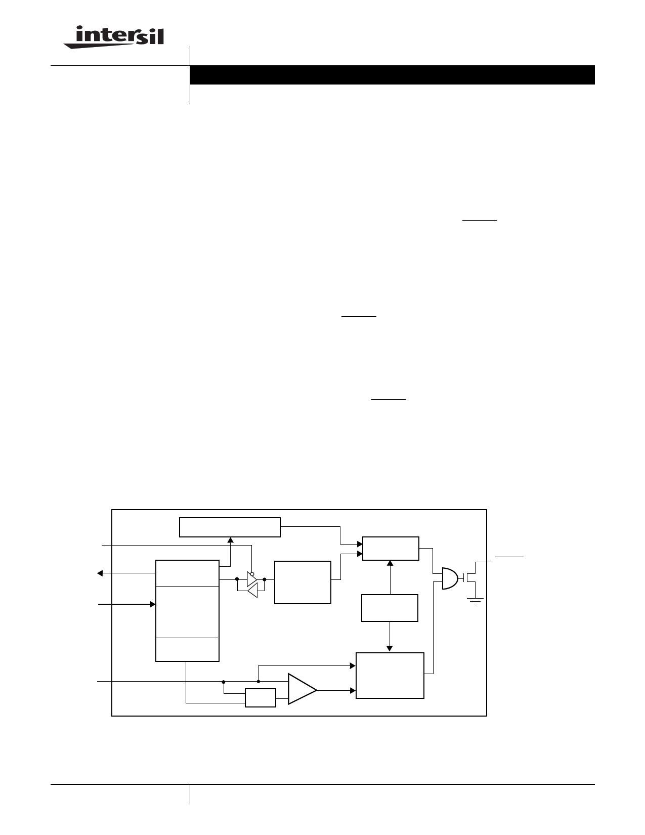
BLOCK DIAGRAM
WP
SDA
SCL
VCC
Watchdog Transition
Detector
Data
Register
Command
Decode &
Control
Logic
VCC Threshold
Reset logic
Control
Register
VTRIP
+
-
DESCRIPTION
These devices combine three popular functions,
Power-on Reset Control, Watchdog Timer, and Supply
Voltage Supervision. This combination lowers system
cost, reduces board space requirements, and
increases reliability.
Applying power to the device activates the power-on
reset circuit which holds RESET/RESET active for a
period of time. This allows the power supply and oscilla-
tor to stabilize before the processor can execute code.
The Watchdog Timer provides an independent
protection mechanism for microcontrollers. When the
microcontroller fails to restart a timer within a select-
able time out interval, the device activates the
RESET/RESET signal. The user selects the interval
from three preset values. Once selected, the interval
does not change, even after cycling the power.
The device’s low VCC detection circuitry protects the
user’s system from low voltage conditions, resetting the
system when VCC falls below the minimum VCC trip
point. RESET/RESET is asserted until VCC returns to
proper operating level and stabilizes. Five industry stan-
dard VTRIP thresholds are available; however, Intersil’s
unique circuits allow the threshold to be reprogrammed
to meet custom requirements, or to fine-tune the thresh-
old for applications requiring higher precision.
Watchdog
Timer Reset
Reset &
Watchdog
Timebase
Power-on and
Low Voltage
Reset
Generation
RESET (X4003)
RESET (X4005)
1 CAUTION: These devices are sensitive to electrostatic discharge; follow proper IC Handling Procedures.
1-888-INTERSIL or 1-888-468-3774 | Intersil (and design) is a registered trademark of Intersil Americas Inc.
Copyright Intersil Americas Inc. 2005-2006. All Rights Reserved
All other trademarks mentioned are the property of their respective owners.
1 page 
X4003, X4005
PRINCIPLES OF OPERATION
Power-on Reset
Application of power to the X4003/X4005 activates a
power-on reset circuit that pulls the RESET/RESET
pin active. This signal provides several benefits.
– It prevents the system microprocessor from starting
to operate with insufficient voltage.
– It prevents the processor from operating prior to
stabilization of the oscillator.
– It allows time for an FPGA to download its configura-
tion prior to initialization of the circuit.
When VCC exceeds the device VTRIP threshold value for
200ms (nominal) the circuit releases RESET/RESET,
allowing the system to begin operation.
Low Voltage Monitoring
During operation, the X4003/X4005 monitors the VCC
level and asserts RESET/RESET if supply voltage falls
below a preset minimum VTRIP. The RESET/RESET
signal prevents the microprocessor from operating in a
power fail or brownout condition. The RESET/RESET
Set VTRIP Level Sequence (VCC = desired VTRIP value)
signal remains active until the voltage drops below 1V.
It also remains active until VCC returns and exceeds
VTRIP for 200ms.
Watchdog Timer
The watchdog timer circuit monitors the microproces-
sor activity by monitoring the SDA and SCL pins. The
microprocessor must toggle the SDA pin HIGH to
LOW periodically, while SCL also toggles from HIGH
to LOW (this is a start bit) followed by a stop condition
prior to the expiration of the watchdog time out period
to prevent a RESET/RESET signal. The state of two
nonvolatile control bits in the control register deter-
mine the watchdog timer period. The microprocessor
can change these watchdog bits, or they may be
“locked” by tying the WP pin HIGH.
Figure 1. Watchdog Restart
.6µs
SCL
.6µs
SDA
Start
Condition
Restart
Stop
Condition
WP
SCL
VP = 15-18V
0 1 2 34 56 7
0 1 23 4 56 7
0 1 23 4 56 7
SDA
A0h
01h
VCC THRESHOLD RESET PROCEDURE
The X4003/X4005 is shipped with a standard VCC
threshold (VTRIP) voltage. This value will not change
over normal operating and storage conditions. How-
ever, in applications where the standard VTRIP is not
exactly right, or if higher precision is needed in the
VTRIP value, the X4003/X4005 threshold may be
adjusted. The procedure is described below, and uses
the application of a nonvolatile control signal.
00h
Setting the VTRIP Voltage
This procedure is used to set the VTRIP to a higher
voltage value. For example, if the current VTRIP is 4.4V
and the new VTRIP is 4.6V, this procedure will directly
make the change. If the new setting is to be lower than
the current setting, then it is necessary to reset the trip
point before setting the new value.
5 FN8113.1
May 11, 2006
5 Page 
X4003, X4005
Serial Read Operations
The read operation allows the master to access the control
register. To conform to the I2C standard, prior to issu-
ing the slave address byte with the R/W bit set to one,
the master must first perform a “dummy” write opera-
tion. The master issues the start condition and the
slave address byte, receives an acknowledge, then
issues the byte address. After acknowledging receipt
of the byte address, the master immediately issues
another start condition and the slave address byte with
the R/W bit set to one. This is followed by an acknowl-
edge from the device and then by the eight bit control
register. The master terminates the read operation by
not responding with an acknowledge and then issuing
a stop condition. Refer to Figure 9 for the address,
acknowledge, and data transfer sequences.
Operational Notes
The device powers-up in the following state:
– The device is in the low power standby state.
– The WEL bit is set to ‘0’. In this state it is not possi-
ble to write to the device.
– SDA pin is the input mode.
RESET/RESET signal is active for tPURST.
Figure 9. Control Register Read Sequence
Signals from
the Master
SDA Bus
Signals from
the Slave
S
t Slave
a
r
Address
t
Byte
Address
S
t
a
r
Slave
Address
t
1 0 11 0 010 1 1 1 1111 1
10 110 011
AA
CC
KK
A
C
K
Data
S
t
o
p
Data Protection
The following circuitry has been included to prevent
inadvertent writes:
– The WEL bit must be set to allow a write operation.
– The proper clock count and bit sequence is required
prior to the stop bit in order to start a nonvolatile
write cycle.
– A three step sequence is required before writing into
the control register to change watchdog timer or
block lock settings.
– The WP pin, when held HIGH, prevents all writes to
the control register.
– Communication to the device is inhibited below the
VTRIP voltage.
– Command to change the control register are termi-
nated if in-progress when RESET/RESET go active.
Symbol Table
WAVEFORM
INPUTS
Must be
steady
May change
from LOW
to HIGH
May change
from HIGH
to LOW
Don’t Care:
Changes
Allowed
N/A
OUTPUTS
Will be
steady
Will change
from LOW
to HIGH
Will change
from HIGH
to LOW
Changing:
State Not
Known
Center Line
is High
Impedance
11 FN8113.1
May 11, 2006
11 Page | ||
| Páginas | Total 18 Páginas | |
| PDF Descargar | [ Datasheet X4003.PDF ] | |
Hoja de datos destacado
| Número de pieza | Descripción | Fabricantes |
| X40010 | Dual Voltage Monitor with Integrated CPU Supervisor | Xicor |
| X40010S8-A | Dual Voltage Monitor with Integrated CPU Supervisor | Xicor |
| X40010S8-B | Dual Voltage Monitor with Integrated CPU Supervisor | Xicor |
| X40010S8-C | Dual Voltage Monitor with Integrated CPU Supervisor | Xicor |
| Número de pieza | Descripción | Fabricantes |
| SLA6805M | High Voltage 3 phase Motor Driver IC. |
Sanken |
| SDC1742 | 12- and 14-Bit Hybrid Synchro / Resolver-to-Digital Converters. |
Analog Devices |
|
DataSheet.es es una pagina web que funciona como un repositorio de manuales o hoja de datos de muchos de los productos más populares, |
| DataSheet.es | 2020 | Privacy Policy | Contacto | Buscar |