|
|
|
PDF ZL50020 Data sheet ( Hoja de datos )
| Número de pieza | ZL50020 | |
| Descripción | Enhanced 2 K Digital Switch | |
| Fabricantes | Zarlink Semiconductor | |
| Logotipo | ||
Hay una vista previa y un enlace de descarga de ZL50020 (archivo pdf) en la parte inferior de esta página. Total 30 Páginas | ||
|
No Preview Available !
www.DataSheet4U.com
ZL50020
Enhanced 2 K Digital Switch
Data Sheet
Features
• 2048 channel x 2048 channel non-blocking digital
Time Division Multiplex (TDM) switch at
8.192 Mbps and 16.384 Mbps or using a
combination of ports running at 2.048, 4.096,
8.192 and 16.384 Mbps
• 32 serial TDM input, 32 serial TDM output
streams
• Output streams can be configured as bi-
directional for connection to backplanes
• Exceptional input clock cycle to cycle variation
tolerance (20 ns for all rates)
• Per-stream input and output data rate conversion
selection at 2.048, 4.096, 8.192 or 16.384 Mbps.
Input and output data rates can differ
• Per-stream high impedance control outputs
(STOHZ) for 16 output streams
• Per-stream input bit delay with flexible sampling
point selection
• Per-stream output bit and fractional bit
advancement
November 2006
Ordering Information
ZL50020GAC 256 Ball PBGA Trays
ZL50020QCC 256 Lead LQFP Trays
ZL50020QCG1 256 Lead LQFP* Trays, Bake &
Drypack
ZL50020GAG2 256 Ball PBGA** Trays, Bake &
Drypack
*Pb Free Matte Tin
**Pb Free Tin/Silver/Copper
-40°C to +85°C
• Per-channel ITU-T G.711 PCM A-Law/µ-Law
Translation
• Four frame pulse and four reference clock outputs
• Three programmable delayed frame pulse outputs
• Input clock: 4.096 MHz, 8.192 MHz, 16.384 MHz
• Input frame pulses:61 ns, 122 ns, 244 ns
• Per-channel constant or variable throughput delay
for frame integrity and low latency applications
• Per Stream (32) Bit Error Rate Test circuits
complying to ITU-O.151
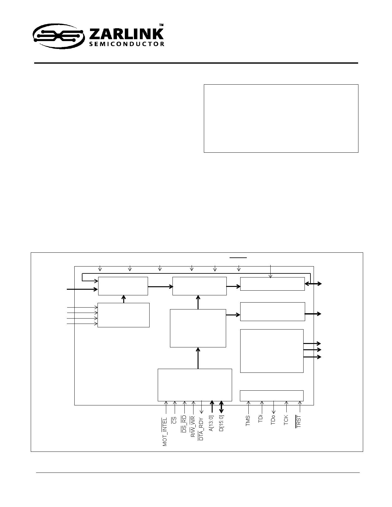
VDD_CORE
VDD_IO
VDD_COREA VDD_IOA
VSS
RESET
ODE
STi[31:0]
FPi
CKi
MODE_4M0
MODE_4M1
S/P Converter
Input Timing
Data Memory
Connection Memory
P/S Converter
Output HiZ
Control
Output Timing
STio[31:0]
STOHZ[15:0]
FPo[3:0]
CKo[3:0]
FPo_OFF[2:0]
Internal Registers &
Microprocessor Interface
Test Port
Figure 1 - ZL50020 Functional Block Diagram
1
Zarlink Semiconductor Inc.
Zarlink, ZL and the Zarlink Semiconductor logo are trademarks of Zarlink Semiconductor Inc.
Copyright 2004-2006, Zarlink Semiconductor Inc. All Rights Reserved.
1 page 
ZL50020
Data Sheet
List of Figures
Figure 1 - ZL50020 Functional Block Diagram . . . . . . . . . . . . . . . . . . . . . . . . . . . . . . . . . . . . . . . . . . . . . . . . . . . . 1
Figure 2 - ZL50020 256-Ball 17 mm x 17 mm PBGA (as viewed through top of package) . . . . . . . . . . . . . . . . . . . 8
Figure 3 - ZL50020 256-Lead 28 mm x 28 mm LQFP (top view). . . . . . . . . . . . . . . . . . . . . . . . . . . . . . . . . . . . . . . 9
Figure 4 - Input Timing when CKIN1 - 0 bits = “10” in the CR . . . . . . . . . . . . . . . . . . . . . . . . . . . . . . . . . . . . . . . . 18
Figure 5 - Input Timing when CKIN1 - 0 bits = “01” in the CR . . . . . . . . . . . . . . . . . . . . . . . . . . . . . . . . . . . . . . . . 18
Figure 6 - Input Timing when CKIN1 - 0 = “00” in the CR . . . . . . . . . . . . . . . . . . . . . . . . . . . . . . . . . . . . . . . . . . . 19
Figure 7 - Output Timing for CKo0 and FPo0 . . . . . . . . . . . . . . . . . . . . . . . . . . . . . . . . . . . . . . . . . . . . . . . . . . . . 20
Figure 8 - Output Timing for CKo1 and FPo1 . . . . . . . . . . . . . . . . . . . . . . . . . . . . . . . . . . . . . . . . . . . . . . . . . . . . 21
Figure 9 - Output Timing for CKo2 and FPo2 . . . . . . . . . . . . . . . . . . . . . . . . . . . . . . . . . . . . . . . . . . . . . . . . . . . . 21
Figure 10 - Output Timing for CKo3 and FPo3 with CKoFPo3SEL1-0=”11” . . . . . . . . . . . . . . . . . . . . . . . . . . . . . 22
Figure 11 - Input Bit Delay Timing Diagram (ST-BUS) . . . . . . . . . . . . . . . . . . . . . . . . . . . . . . . . . . . . . . . . . . . . . . 23
Figure 12 - Input Bit Sampling Point Programming . . . . . . . . . . . . . . . . . . . . . . . . . . . . . . . . . . . . . . . . . . . . . . . . 24
Figure 13 - Input Bit Delay and Factional Sampling Point . . . . . . . . . . . . . . . . . . . . . . . . . . . . . . . . . . . . . . . . . . . 25
Figure 14 - Output Bit Advancement Timing Diagram (ST-BUS) . . . . . . . . . . . . . . . . . . . . . . . . . . . . . . . . . . . . . . 26
Figure 15 - Output Fractional Bit Advancement Timing Diagram (ST-BUS) . . . . . . . . . . . . . . . . . . . . . . . . . . . . . 27
Figure 16 - Channel Switching External High Impedance Control Timing . . . . . . . . . . . . . . . . . . . . . . . . . . . . . . . 28
Figure 17 - Data Throughput Delay for Variable Delay . . . . . . . . . . . . . . . . . . . . . . . . . . . . . . . . . . . . . . . . . . . . . 29
Figure 18 - Data Throughput Delay for Constant Delay. . . . . . . . . . . . . . . . . . . . . . . . . . . . . . . . . . . . . . . . . . . . . 30
Figure 19 - Timing Parameter Measurement Voltage Levels . . . . . . . . . . . . . . . . . . . . . . . . . . . . . . . . . . . . . . . . . 62
Figure 20 - Motorola Non-Multiplexed Bus Timing - Read Access . . . . . . . . . . . . . . . . . . . . . . . . . . . . . . . . . . . . 63
Figure 21 - Motorola Non-Multiplexed Bus Timing - Write Access. . . . . . . . . . . . . . . . . . . . . . . . . . . . . . . . . . . . . 64
Figure 22 - Intel Non-Multiplexed Bus Timing - Read Access . . . . . . . . . . . . . . . . . . . . . . . . . . . . . . . . . . . . . . . . 65
Figure 23 - Intel Non-Multiplexed Bus Timing - Write Access . . . . . . . . . . . . . . . . . . . . . . . . . . . . . . . . . . . . . . . . 66
Figure 24 - JTAG Test Port Timing Diagram . . . . . . . . . . . . . . . . . . . . . . . . . . . . . . . . . . . . . . . . . . . . . . . . . . . . . 67
Figure 25 - Frame Pulse Input and Clock Input Timing Diagram (ST-BUS). . . . . . . . . . . . . . . . . . . . . . . . . . . . . . 69
Figure 26 - Frame Pulse Input and Clock Input Timing Diagram (GCI-Bus) . . . . . . . . . . . . . . . . . . . . . . . . . . . . . 69
Figure 27 - ST-BUS Input Timing Diagram when Operated at 2, 4, 8 Mbps . . . . . . . . . . . . . . . . . . . . . . . . . . . . . 70
Figure 28 - ST-BUS Input Timing Diagram when Operated at 16 Mbps . . . . . . . . . . . . . . . . . . . . . . . . . . . . . . . . 71
Figure 29 - GCI-Bus Input Timing Diagram when Operated at 2, 4, 8 Mbps . . . . . . . . . . . . . . . . . . . . . . . . . . . . . 71
Figure 30 - GCI-Bus Input Timing Diagram when Operated at 16 Mbps . . . . . . . . . . . . . . . . . . . . . . . . . . . . . . . . 72
Figure 31 - ST-BUS Output Timing Diagram when Operated at 2, 4, 8 or 16 Mbps . . . . . . . . . . . . . . . . . . . . . . . 73
Figure 32 - GCI-Bus Output Timing Diagram when Operated at 2, 4, 8 or 16 Mbps . . . . . . . . . . . . . . . . . . . . . . . 73
Figure 33 - Serial Output and External Control . . . . . . . . . . . . . . . . . . . . . . . . . . . . . . . . . . . . . . . . . . . . . . . . . . . 74
Figure 34 - Output Drive Enable (ODE) . . . . . . . . . . . . . . . . . . . . . . . . . . . . . . . . . . . . . . . . . . . . . . . . . . . . . . . . . 74
Figure 35 - Input and Output Frame Boundary Offset . . . . . . . . . . . . . . . . . . . . . . . . . . . . . . . . . . . . . . . . . . . . . . 75
Figure 36 - FPo0 and CKo0 Timing Diagram. . . . . . . . . . . . . . . . . . . . . . . . . . . . . . . . . . . . . . . . . . . . . . . . . . . . . 76
Figure 37 - FPo1 and CKo1 Timing Diagram. . . . . . . . . . . . . . . . . . . . . . . . . . . . . . . . . . . . . . . . . . . . . . . . . . . . . 77
Figure 38 - FPo2 and CKo2 Timing Diagram. . . . . . . . . . . . . . . . . . . . . . . . . . . . . . . . . . . . . . . . . . . . . . . . . . . . . 78
Figure 39 - FPo3 and CKo3 Timing Diagram. . . . . . . . . . . . . . . . . . . . . . . . . . . . . . . . . . . . . . . . . . . . . . . . . . . . . 79
Figure 40 - Output Timing (ST-BUS Format) . . . . . . . . . . . . . . . . . . . . . . . . . . . . . . . . . . . . . . . . . . . . . . . . . . . . . 80
5
Zarlink Semiconductor Inc.
5 Page 
ZL50020
Data Sheet
PBGA Pin
Number
K3
LQFP Pin
Number
234
L4 238
L3 239
M3 240
G5 212
B12, B13,
C10, C11,
F13, G4,
K12, C12,
G3, D12,
B14, C13
80, 105,
150, 151,
152, 153,
210, 149
144, 107,
148, 208
Pin Name
TMS
TCK
TRST
TDi
TDo
IC_Open
IC_GND
Description
Test Mode Select (5 V-Tolerant Input with Internal Pull-up)
JTAG signal that controls the state transitions of the TAP controller.
This pin is pulled high by an internal pull-up resistor when it is not
driven.
Test Clock (5 V-Tolerant Schmitt-Triggered Input with Internal
Pull-up)
Provides the clock to the JTAG test logic.
Test Reset (5 V-Tolerant Input with Internal Pull-up)
Asynchronously initializes the JTAG TAP controller by putting it in
the Test-Logic-Reset state. This pin should be pulsed low during
power-up to ensure that the device is in the normal functional
mode. When JTAG is not being used, this pin should be pulled low
during normal operation.
Test Serial Data In (5 V-Tolerant Input with Internal Pull-up)
JTAG serial test instructions and data are shifted in on this pin.
This pin is pulled high by an internal pull-up resistor when it is not
driven.
Test Serial Data Out (5 V-Tolerant Three-state Output)
JTAG serial data is output on this pin on the falling edge of TCK.
This pin is held in high impedance state when JTAG is not
enabled.
Internal Test Mode (5 V-Tolerant Input with Internal Pull-down)
These pins may be left unconnected.
Internal Test Mode Enable (5 V-Tolerant Input)
These pins MUST be low.
11
Zarlink Semiconductor Inc.
11 Page | ||
| Páginas | Total 30 Páginas | |
| PDF Descargar | [ Datasheet ZL50020.PDF ] | |
Hoja de datos destacado
| Número de pieza | Descripción | Fabricantes |
| ZL50020 | Enhanced 2 K Digital Switch | Zarlink Semiconductor |
| ZL50021 | Enhanced 4 K Digital Switch | Zarlink Semiconductor |
| ZL50022 | Enhanced 4 K Digital Switch | Zarlink Semiconductor |
| ZL50023 | Enhanced 4 K Digital Switch | Zarlink Semiconductor |
| Número de pieza | Descripción | Fabricantes |
| SLA6805M | High Voltage 3 phase Motor Driver IC. |
Sanken |
| SDC1742 | 12- and 14-Bit Hybrid Synchro / Resolver-to-Digital Converters. |
Analog Devices |
|
DataSheet.es es una pagina web que funciona como un repositorio de manuales o hoja de datos de muchos de los productos más populares, |
| DataSheet.es | 2020 | Privacy Policy | Contacto | Buscar |