|
|
|
PDF ZL30410 Data sheet ( Hoja de datos )
| Número de pieza | ZL30410 | |
| Descripción | Multi-service Line Card PLL | |
| Fabricantes | Zarlink Semiconductor | |
| Logotipo | ||
Hay una vista previa y un enlace de descarga de ZL30410 (archivo pdf) en la parte inferior de esta página. Total 30 Páginas | ||
|
No Preview Available !
www.DataSheet4U.com
ZL30410
Multi-service Line Card PLL
Data Sheet
Features
• Generates clocks for OC-3, STM-1, DS3, E3,
DS2, DS1, E1, 19.44 MHz and ST-BUS
• Meets jitter generation requirements for STM-1,
OC-3, DS3, E3, J2 (DS2), E1 and DS1 interfaces
• Compatible with GR-253-CORE SONET stratum
3 and G.813 SEC timing compliant clocks
• Provides “hit-less” reference switching
• Detects frequency of both reference clocks and
synchronizes to any combination of 8 kHz, 1.544
MHz, 2.048 MHz and 19.44 MHz reference
frequencies
• Continuously monitors both references for
frequency accuracy exceeding ±12 ppm
• Holdover accuracy of 70x10 -12 meets GR-1244
Stratum 3E and ITU-T G.812 requirements
• Meets requirements of G.813 Option 1 for SDH
Equipment Clocks (SEC) and GR-1244 for
Stratum 4E and Stratum 4 Clocks
• 3.3V power supply
Applications
• Line Card synchronization for SDH, SONET, DS3,
E3, J2 (DS2), E1 and DS1 interfaces
• Timing card synchronization for SDH and PDH
Network Elements
November 2003
Ordering Information
ZL30410QCC
80 Pin LQFP
-40°C to 85°C
• Clock generation for ST-BUS and GCI timing
Description
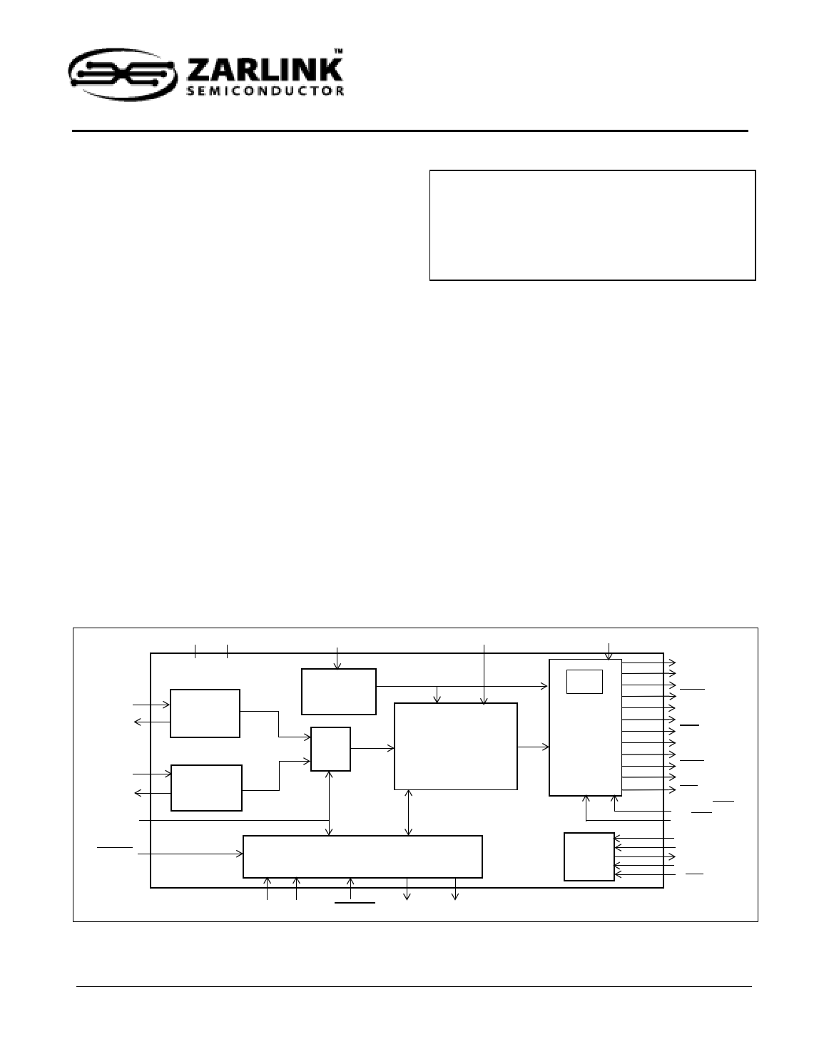
The ZL30410 is a Multi-service Line Card
Phase-Locked Loop designed to generate multiple
clocks for SONET, SDH and PDH equipment including
timing for ST-BUS and GCI interfaces.
The ZL30410 operates in NORMAL (LOCKED),
HOLDOVER and FREE-RUN modes to ensure that in
the presence of jitter and interruptions to the reference
signals, the generated clocks meet international
standards. The filtering characteristics of the PLL are
hardware pin selectable and they do not require any
external adjustable components. The ZL30410 uses an
external 20 MHz Master Clock Oscillator to provide a
stable timing source for the HOLDOVER operation.
PRI
PRIOR
SEC
SECOR
RefSel
RESET
VDD GND
Primary
Acquisition
PLL
Secondary
Acquisition
PLL
C20i
Master Clock
Frequency
Calibration
MUX
FCS
Core PLL
OE
APLL
Clock
Synthesizer
Control State Machine
JTAG
IEEE
1149.1a
MS1 MS2 RefAlign LOCK HOLDOVER
Figure 1 - Functional Block Diagram
Zarlink Semiconductor US Patent No. 5,602,884, UK Patent No. 0772912,
France Brevete S.G.D.G. 0772912; Germany DBP No. 69502724.7-08
1
Zarlink Semiconductor Inc.
Zarlink, ZL and the Zarlink Semiconductor logo are trademarks of Zarlink Semiconductor Inc.
Copyright 2003, Zarlink Semiconductor Inc. All Rights Reserved.
C155P/N
C34/C44
C19o
C16o
C8o
C6o
C4o
C2o
C1.5o
F16o
F8o
F0o
E3DS3/OC3
E3/DS3
Tclk
Tdi
Tdo
Tms
Trst
07
1 page 
ZL30410
Data Sheet
Pin Description (continued)
Pin #
Name
21 E3DS3/OC3
22 E3/DS3
23 SEC
24 PRI
25 GND
26 IC
27 GND
28 AVDD
29 VDD
30 C155N
31 C155P
32 GND
33 NC
34 Tdo
35 Tms
Description
E3DS3 or OC3 Selection (Input). In Hardware Control, a logic low on this pin
enables the C155P/N outputs (pin 30 and pin 31) and sets the C34/C44 output
(pin 53) to provide C8 or C11 clocks. Logic high at this input disables the C155
clock outputs (high impedance) and sets C34/C44 output to provide C34 and
C44 clocks.
E3 or DS3 Selection (Input). In Hardware Control, when the E3DS3/OC3 pin
is set high, logic low on E3/DS3 pin selects a 44.736 MHz clock on C34/C44
output and logic high selects 34.368 MHz clock. When E3DS3/OC3 pin is set
low, logic low on E3/DS3 pin selects 11.184 MHz clock on C34/C44 output and
logic high selects 8.592 MHz clock.
Secondary Reference (Input). This input is used as a secondary reference
source for synchronization. The ZL30410 can synchronize to the falling edge
of the 8 kHz, 1.544 MHz or 2.048 MHz clocks and the rising edge of the 19.44
MHz clock. In Hardware Control, selection of the input reference is based upon
the RefSel control input. This pin is internally pulled up to VDD.
Primary Reference (Input). This input is used as a primary reference source
for synchronization. The ZL30410 can synchronize to the falling edge of the 8
kHz, 1.544 MHz or 2.048 MHz clocks and the rising edge of the 19.44 MHz
clock. In Hardware Control, selection of the input reference is based upon the
RefSel control input. This pin is internally pulled up to VDD.
Ground.
Internal Connection. Leave unconnected.
Ground.
Positive Analog Power Supply. Connect this pin to VDD.
Positive Power Supply.
Clock 155.52MHz (LVDS output). Differential outputs for the 155.52 MHz
clock. These outputs are enabled by applying logic low to E3DS3/OC3 input or
they can be disabled by applying logic high. In the disabled state the LVDS
outputs are internally terminated with an integrated 100Ω resistor (two 50Ω
resistors connected in series). The middle point of these resistors is internally
biased from a 1.25V LVDS bias source.
Ground.
No internal bonding Connection. Leave unconnected.
IEEE1149.1a Test Data Output (CMOS output). JTAG serial data is output on
this pin on the falling edge of Tclk clock. If not used, this pin should be left
unconnected.
IEEE1149.1a Test Mode Selection (3.3 V input). JTAG signal that controls the
state transition on the TAP controller. This pin is internally pulled up to VDD. If
not used, this pin should be left unconnected.
5
Zarlink Semiconductor Inc.
5 Page 
ZL30410
Data Sheet
- C155 : 155.52 MHz clock with nominal 50% duty cycle.
The ZL30410 provides the following frame pulses (see Figure 15 "ST-BUS and GCI Output Timing" for details). All
frame pulses have the same 125µs period (8kHz frequency):
- F0o
: 244 ns wide, logic low frame pulse
- F8o
: 122 ns wide, logic high frame pulse
- F16o : 61 ns wide, logic low frame pulse
The combination of two pins, E3DS3/OC3 and E3/DS3, controls the selection of different clock configurations.
When the E3DS3/OC3 pin is high then the C155o (155.52 MHz) clock is disabled and the C34/44 clock is output at
its nominal frequency. The logic level on the E3/DS3 input determines if the output clock on the C34/44 output is
34.368 MHz (E3) or 44.736 MHz (DS3) (see Figure 4, “C34/C44, C155o Clock Generation Options,” on page 11 for
details).
C34/44 Output
E3DS3/OC3
01
0 11.184 44.736
1 8.592 34.368
C155 Output
E3DS3/OC3
01
155.52 disabled
active
Figure 4 - C34/C44, C155o Clock Generation Options
All clocks and frame pulses (except the C155) are output with CMOS logic levels. The C155 clock (155.52 MHz) is
output in a standard LVDS format.
2.4 Control State Machine
2.4.1 Clock Modes
The ZL30410 supports three Clock Modes: Free-run, Normal (Locked) and Holdover. All Clock Modes are defined
in the international standards e.g.: G.813, GR-1244-CORE and GR-253-CORE and they are supported by a
corresponding state in the ZL30410 Control State Machine.
2.4.2 ZL30410 State Machine
The ZL30410 Control State Machine is a combination of many internal states supporting the three mandatory clock
modes: Free-run, Normal and Holdover. A simplified state machine diagram that is shown in Figure 5 includes
these three states which are complemented by two additional states: Reset and Auto Holdover. These two
additional states are critical to the ZL30410 operation under changing external conditions.
11
Zarlink Semiconductor Inc.
11 Page | ||
| Páginas | Total 30 Páginas | |
| PDF Descargar | [ Datasheet ZL30410.PDF ] | |
Hoja de datos destacado
| Número de pieza | Descripción | Fabricantes |
| ZL30410 | Multi-service Line Card PLL | Zarlink Semiconductor |
| ZL30414 | SONET/SDH Clock Multiplier PLL | Zarlink Semiconductor |
| ZL30415 | SONET/SDH Clock Multiplier PLL | Zarlink Semiconductor |
| ZL30416 | SONET/SDH Clock Multiplier PLL | Zarlink Semiconductor |
| Número de pieza | Descripción | Fabricantes |
| SLA6805M | High Voltage 3 phase Motor Driver IC. |
Sanken |
| SDC1742 | 12- and 14-Bit Hybrid Synchro / Resolver-to-Digital Converters. |
Analog Devices |
|
DataSheet.es es una pagina web que funciona como un repositorio de manuales o hoja de datos de muchos de los productos más populares, |
| DataSheet.es | 2020 | Privacy Policy | Contacto | Buscar |