|
|
|
PDF NM24C16U Data sheet ( Hoja de datos )
| Número de pieza | NM24C16U | |
| Descripción | (NM24C16U / NM24C17U) 16K-Bit Serial EEPROM 2-Wire Bus Interface | |
| Fabricantes | Fairchild Semiconductor | |
| Logotipo | ||
Hay una vista previa y un enlace de descarga de NM24C16U (archivo pdf) en la parte inferior de esta página. Total 13 Páginas | ||
|
No Preview Available !
www.DataSheet4U.com
August 1999
NM24C16U/NM24C17U
16K-Bit Serial EEPROM
2-Wire Bus Interface
General Description
The NM24C16U/17U devices are 16K (16,384) bit serial interface
CMOS EEPROMs (Electrically Erasable Programmable Read-
Only Memory). These devices fully conform to the Standard I2C™
2-wire protocol which uses Clock (SCL) and Data I/O (SDA) pins
to synchronously clock data between the "master" (for example a
microprocessor) and the "slave" (the EEPROM device). In addi-
tion, the serial interface allows a minimal pin count packaging
designed to simplify PC board layout requirements and offers the
designer a variety of low voltage and low power options.
NM24C17U incorporates a hardware "Write Protect" feature, by
which, the upper half of the memory can be disabled against
programming by connecting the WP pin to VCC. This section of
memory then effectively becomes a ROM (Read-Only Memory)
and can no longer be programmed as long as WP pin is connected
to VCC.
Fairchild EEPROMs are designed and tested for applications requir-
ing high endurance, high reliability and low power consumption for a
continuously reliable non-volatile solution for all markets.
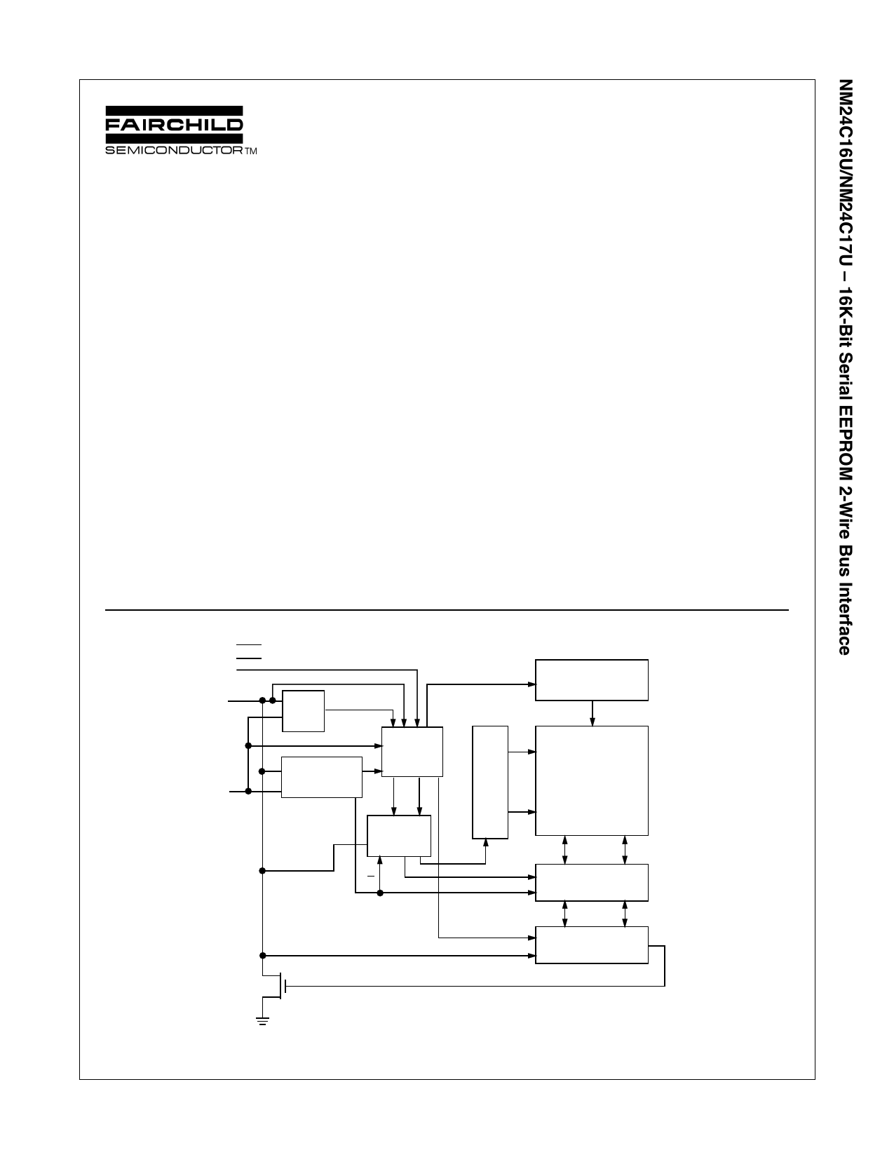
Block Diagram
VCC
VSS
WP
SDA
SCL
START
STOP
LOGIC
SLAVE ADDRESS
REGISTER &
COMPARATOR
CONTROL
LOGIC
Functions
I I2C™ compatible interface
I 4,096 bits organized as 512 x 8
I Extended 2.7V – 5.5V operating voltage
I 100 KHz or 400 KHz operation
I Self timed programming cycle (6ms typical)
I "Programming complete" indicated by ACK polling
I NM24C17U: Memory "Upper Block" Write Protect pin
Features
I The I2C™ interface allows the smallest I/O pincount of any
EEPROM interface
I 16 byte page write mode to minimize total write time per byte
I Typical 200µA active current (ICCA)
I Typical 1µA standby current (ISB) for "L" devices and 0.1µA
standby current for "LZ" devices
I Endurance: Up to 1,000,000 data changes
I Data retention greater than 40 years
H.V. GENERATION
TIMING &CONTROL
XDEC
E2PROM
ARRAY
WORD
ADDRESS
COUNTER
R/W YDEC
CK
DIN
DATA REGISTER
DOUT
I2C™ is a registered trademark of Philips Electronics N.V.
© 1999 Fairchild Semiconductor Corporation
NM24C16U/17U Rev. B.1
1
DS800010-1
www.fairchildsemi.com
1 page 
AC Conditions of Test
Input Pulse Levels
Input Rise and Fall Times
VCC x 0.1 to VCC x 0.9
10 ns
Input & Output Timing Levels VCC x 0.5
Output Load
1 TTL Gate and CL = 100 pF
Read and Write Cycle Limits (Standard and Low VCC Range 2.7V - 5.5V)
Symbol
Parameter
100 KHz
Min Max
400 KHz
Min Max
fSCL SCL Clock Frequency
TI Noise Suppression Time Constant at
SCL, SDA Inputs (Minimum VIN
Pulse width)
100
100
400
50
tAA SCL Low to SDA Data Out Valid 0.3 3.5 0.1 0.9
tBUF Time the Bus Must Be Free before
a New Transmission Can Start
4.7
1.3
tHD:STA
tLOW
tHIGH
tSU:STA
Start Condition Hold Time
Clock Low Period
Clock High Period
Start Condition Setup Time
(for a Repeated Start Condition)
4.0
4.7
4.0
4.7
0.6
1.5
0.6
0.6
tHD:DAT
Data in Hold Time
0
0
tSU:DAT
Data in Setup Time
250
100
tR SDA and SCL Rise Time
1 0.3
tF SDA and SCL Fall Time
300 300
tSU:STO
Stop Condition Setup Time
4.7
0.6
tDH Data Out Hold Time
300
50
tWR
(Note 3)
Write Cycle Time - NM24C16U/17U
- NM24C16U/17UL, NM24C16U/17ULZ
10
15
10
15
Units
KHz
ns
µs
µs
µs
µs
µs
µs
µs
ns
µs
ns
µs
ns
ms
Note 3: The write cycle time (tWR) is the time from a valid stop condition of a write sequence to the end of the internal erase/program cycle. During the write cycle, the
NM24C16U/17U bus interface circuits are disabled, SDA is allowed to remain high per the bus-level pull-up resistor, and the device does not respond to its slave address.
NM24C16U/17U Rev. B.1
5
www.fairchildsemi.com
5 Page 
Read Operations
Read operations are initiated in the same manner as write
operations, with the exception that the R/W bit of the slave
address is set to a one. There are three basic read operations:
current address read, random read, and sequential read.
Current Address Read
Internally the NM24C16U/17U contains an address counter that
maintains the address of the last byte accessed, incremented by
one. Therefore, if the last access (either a read or write) was to
address n, the next read operation would access data from
address n + 1. Upon receipt of the slave address with R/W set to
one, the NM24C16U/17U issues an acknowledge and transmits
the eight bit byte. The master will not acknowledge the transfer
but does generate a stop condition, and therefore the NM24C16U/
17U discontinues transmission. Refer to Figure 8 for the se-
quence of address, acknowledge and data transfer.
Random Read
Random read operations allow the master to access any memory
location in a random manner. Prior to issuing the slave address
with the R/W bit set to one, the master must first perform a
“dummy” write operation. The master issues the start condition,
slave address and then the byte address it is to read. After the
byte address acknowledge, the master immediately reissues the
start condition and the slave address with the R/W bit set to one.
This will be followed by an acknowledge from the NM24C16U/17U
and then by the eight bit data. The master will not acknowledge the
transfer but does generate the stop condition, and therefore the
NM24C16U/17U discontinues transmission. Refer to Figure 9 for
the address, acknowledge and data transfer sequence.
Sequential Read
Sequential reads can be initiated as either a current address read
or random access read. The first word is transmitted in the same
manner as the other read modes; however, the master now
responds with an acknowledge, indicating it requires additional
data. The NM24C16U/17U continues to output data for each
acknowledge received. The read operation is terminated by the
master not responding with an acknowledge or by generating a
stop condition.
The data output is sequential, with the data from address n
followed by the data from n + 1. The address counter for read
operations increments all word address bits, allowing the entire
memory contents to be serially read during one operation. After
the entire memory has been read, the counter "rolls over" and the
NM24C16U/17U continues to output data for each acknowledge
received. Refer to Figure 10 for the address, acknowledge, and
data transfer sequence.
Current Address Read (Figure 8)
Bus Activity:
Master
S
T
A
R
T
SDA Line
Bus Activity:
NM24C16U/17U
Random Read (Figure 9)
S
T
Bus Activity:
Master
A
R
T
SLAVE
ADDRESS
SLAVE
ADDRESS
S
T
O
P
A NO
C DATA
K
A
C
K
DS800010-17
WORD
ADDRESS
S
T
A SLAVE
R ADDRESS
T
S
T
O
P
SDA Line
Bus Activity:
NM24C16U/17U
AA
CC
KK
A NO
C
DATA n
A
KC
K
DS800010-18
Sequential Read (Figure 10)
Bus Activity:
Master
Slave
Address
SDA Line
Bus Activity:
NM24C16U/17U
A
C
K
DATA n +1
A AA
C CC
K KK
DATA n +1
DATA n + 2
S
T
O
P
DATA n + x
NO
A
C
K
DS800010-19
NM24C16U/17U Rev. B.1
11
www.fairchildsemi.com
11 Page | ||
| Páginas | Total 13 Páginas | |
| PDF Descargar | [ Datasheet NM24C16U.PDF ] | |
Hoja de datos destacado
| Número de pieza | Descripción | Fabricantes |
| NM24C16 | 16K-Bit Standard 2-Wire Bus Interface Serial EEPROM | Fairchild |
| NM24C16U | (NM24C16U / NM24C17U) 16K-Bit Serial EEPROM 2-Wire Bus Interface | Fairchild Semiconductor |
| Número de pieza | Descripción | Fabricantes |
| SLA6805M | High Voltage 3 phase Motor Driver IC. |
Sanken |
| SDC1742 | 12- and 14-Bit Hybrid Synchro / Resolver-to-Digital Converters. |
Analog Devices |
|
DataSheet.es es una pagina web que funciona como un repositorio de manuales o hoja de datos de muchos de los productos más populares, |
| DataSheet.es | 2020 | Privacy Policy | Contacto | Buscar |