|
|
|
PDF AD71028 Data sheet ( Hoja de datos )
| Número de pieza | AD71028 | |
| Descripción | Dual Digital BTSC Encoder | |
| Fabricantes | Analog Devices | |
| Logotipo | ||
Hay una vista previa y un enlace de descarga de AD71028 (archivo pdf) en la parte inferior de esta página. Total 20 Páginas | ||
|
No Preview Available !
www.DataSheet4U.com
FEATURES
2 complete independent BTSC encoders
Pilot tone generator
Includes subcarrier modulation
Typical 23 dB to 27 dB separation, 16 dB minimum
Signal bandwidth of 14 kHz
Phat-StereoTM algorithm for stereo image enhancement
Dialog enhancement function for playing wide dynamic
range video sources over built-in TV speakers
Includes L-R dual-band compressor
SPI® port for control of modes and effects
Differential output for optimum performance
DAC performance: 92 dB dynamic range, –92 dB THD+N
Output level control for setting aural carrier deviation
Flexible serial data port with right-justified, left-justified,
I2S compatible, and DSP serial port modes
48-lead LQFP plastic package
APPLICATIONS
Digital set-top box BTSC encoder
Dual Digital BTSC Encoder
with Integrated DAC
AD71028
PRODUCT OVERVIEW
The AD71028 dual digital BTSC encoder provides two complete
digital BTSC encoder channels, including the pilot-tone
generation and subcarrier mixing functions. Two built-in high
performance DACs are provided to output the BTSC baseband
composite signal. The output of the AD71028 can be connected
with minimal external circuitry to the input of a 4.5 MHz aural
FM modulator.
In addition to the BTSC encoders, the AD71028 also includes a
stereo image enhancement function, Phat Stereo, to increase the
sense of spaciousness available from closely spaced TV
loudspeakers. A dialog enhancement algorithm is also included
to solve the problem of playing wide dynamic range sources
over limited-performance TV speakers and amplifiers. An
extensive SPI port allows click-free parameter updates.
The AD71028 also includes ADI’s patented multibit Σ-∆ DAC
architecture. This architecture provides 92 dB SNR and THD+N
of –92 dB.
SERIAL 3
INPUT A
CLOCK
SIGNAL
GROUP
SERIAL 3
INPUT B
SPI I/O
GROUP
4
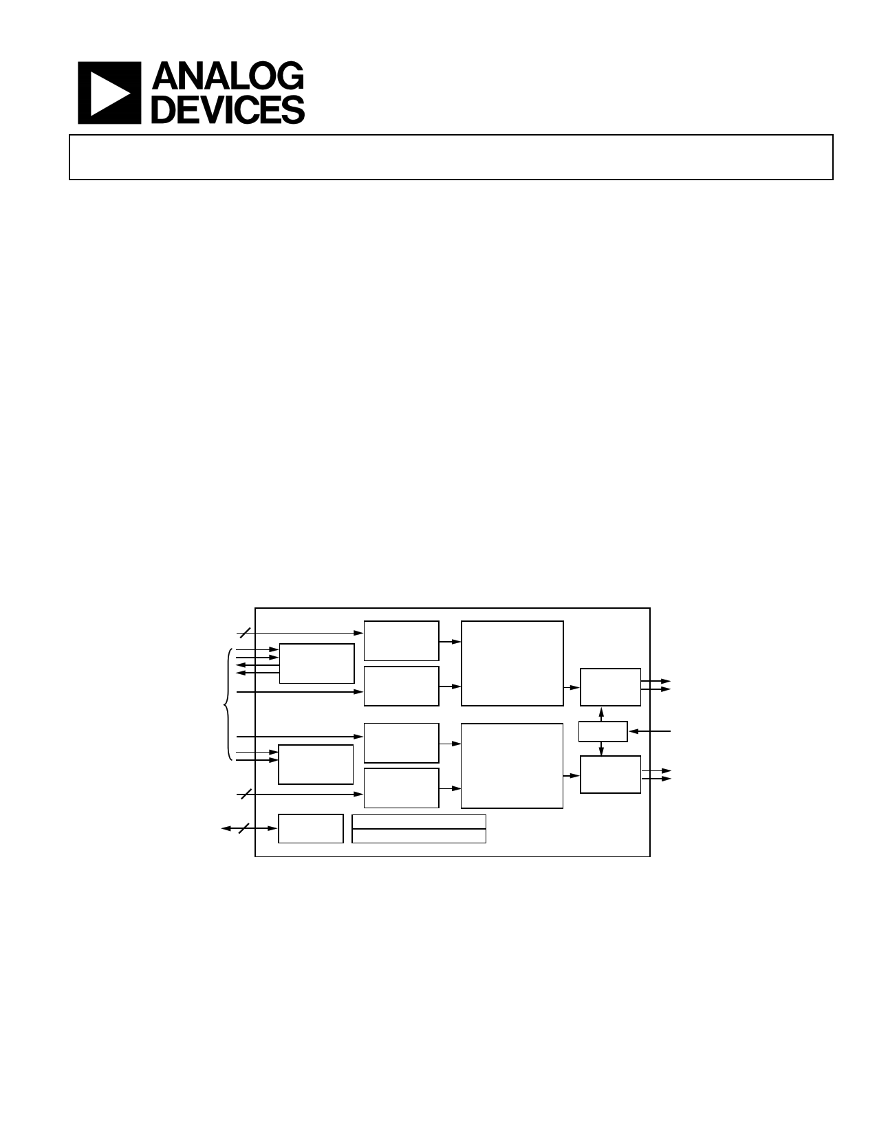
FUNCTIONAL BLOCK DIAGRAM
PLL DIVIDERS
SERIAL
INPUT
CLOCK
DOUBLER
BTSC
ENCODER
CORE A
PLL DIVIDERS
CLOCK
DOUBLER
SERIAL
INPUT
BTSC
ENCODER
CORE B
SPI PORT
CONTROL REGISTERS
PARAMETER RAM
Figure 1. Functional Block Diagram
DAC
BIAS
DAC
AD71028
BTSC
ENCODED
OUTPUT A
ANALOG
BIAS
BTSC
ENCODED
OUTPUT B
Rev. 0
Information furnished by Analog Devices is believed to be accurate and reliable.
However, no responsibility is assumed by Analog Devices for its use, nor for any
infringements of patents or other rights of third parties that may result from its use.
Specifications subject to change without notice. No license is granted by implication
or otherwise under any patent or patent rights of Analog Devices. Trademarks and
registered trademarks are the property of their respective owners.
One Technology Way, P.O. Box 9106, Norwood, MA 02062-9106, U.S.A.
Tel: 781.329.4700
www.analog.com
Fax: 781.326.8703 © 2004 Analog Devices, Inc. All rights reserved.
1 page 
ABSOLUTE MAXIMUM RATINGS
Table 7. AD71028 Stress Ratings
Parameter
Min Max
DVDD to DGND
ODVDD to DGND
AVDD to AGND
–0.3
–0.3
–0.3
+6
+6
+6
Digital Inputs
Analog Inputs
AGND to DGND
Reference Voltage
Maximum Junction
Temperature
Storage Temperature
DGND – 0.3
AGND – 0.3
–0.3
DVDD + 0.3
AVDD + 0.3
+0.3
(AVDD + 0.3)/2
125
Range
–65 +150
Soldering
300
10
Unit
V
V
V
V
V
V
V
°C
°C
°C
sec
AD71028
Table 8. Package Characteristics (48-Lead LQFP)
Parameter
Min Typ Max
θJA Thermal Resistance
[Junction-to-Ambient]
72
θJC Thermal Resistance
[Junction-to-Case]
19.5
Unit
°C/W
°C/W
Stresses above those listed under Absolute Maximum Ratings
may cause permanent damage to the device. This is a stress
rating only; functional operation of the device at these or any
other conditions above those listed in the operational sections
of this specification is not implied. Exposure to absolute
maximum rating conditions for extended periods may affect
device reliability.
ESD CAUTION
ESD (electrostatic discharge) sensitive device. Electrostatic charges as high as 4000 V readily accumulate on
the human body and test equipment and can discharge without detection. Although this product features
proprietary ESD protection circuitry, permanent damage may occur on devices subjected to high energy
electrostatic discharges. Therefore, proper ESD precautions are recommended to avoid performance
degradation or loss of functionality.
Rev. 0 | Page 5 of 20
5 Page 
PHASE LINEARITY OF THE EXTERNAL ANALOG
FILTER
If the time alignment of the pilot to the carrier signal is not
close to 0 degrees, a loss of separation can occur. This means
that the external analog low-pass filter should be a linear-phase
design to provide constant group delay over the range from dc
to 50 kHz. Bessel filters are recommended for this application.
Figure 12 shows a recommended design for these filters.
INPUT LEVELS
The maximum input level to the AD71028 changes across
frequency. Table 10 shows the maximum allowable input level
for different frequencies. These values are part of the BTSC
specification and are not a function of this chip.
Table 10. Maximum Input Levels to the BTSC Encoder
across Frequency
Frequency (Hz)
Maximum Input Level (dBFS)
20 to 1000
0 dB
1600
–1 dB
2500
–3 dB
3150
–5 dB
5000
–8 dB
8000
–11 dB
12500
–15 dB
CLOCK RELATIONSHIPS
In an MPEG receiver architecture, all clocks are typically
generated from a 27 MHz master clock. The following integer
relationships are found between the clocks, with Fh =
15.734 kHz:
a) 27 MHz/Fh = 1716 = 2 × 2 × 3 × 11 × 13
b) Fh/2 = F /(5color_subcarrier × 7 × 13)
c) 27 MHz/Fcolor_subcarrier = (5 × 7)/(2 × 2 × 2 × 3 × 11)
d) 27 MHz/48 kHz = 1125/2
AD71028
The AD71028 contains a clock doubler circuit that may be used
to generate an internal 512 × fS clock when the external clock is
256 × fS. The clock mode is set by connecting the DOUBLE pin
either high or low. This pin should be tied either high or low
and should not be changed after power-up.
The AD71028 requires a master clock at either 256 × 48 kHz
(12.288 MHz) when DOUBLE = 1 or 512 × 48 kHz
(24.576 MHz) when DOUBLE = 0. In some cases, this signal is
provided by the MPEG decoder chip itself. In other cases, only
the 27 MHz video clock may be available. In this case, the
AD71028 provides on-chip dividers to interface to an external
PLL such as the 74HC4046. Figure 4 shows the circuit to
accomplish this. The 27 MHz clock is applied to the AD71028
and divided down by 1125, producing a signal at 24 kHz. The
PLL oscillator output is divided down by 512, producing a
24 kHz output (when locked). These two signals are applied to
the phase-comparator inputs of the external PLL. Note that the
divided-down 27 MHz signal looks like a pulse with a duration
of one master clock, and therefore only edge-triggered phase
detectors should be used.
27MHz IN
AD71028
DIVIDE-BY-1125
74HC4046
DIVIDE-BY-512
DSP
Figure 4. PLL Connections for 27 MHz Master Clock
Rev. 0 | Page 11 of 20
11 Page | ||
| Páginas | Total 20 Páginas | |
| PDF Descargar | [ Datasheet AD71028.PDF ] | |
Hoja de datos destacado
| Número de pieza | Descripción | Fabricantes |
| AD71028 | Dual Digital BTSC Encoder | Analog Devices |
| Número de pieza | Descripción | Fabricantes |
| SLA6805M | High Voltage 3 phase Motor Driver IC. |
Sanken |
| SDC1742 | 12- and 14-Bit Hybrid Synchro / Resolver-to-Digital Converters. |
Analog Devices |
|
DataSheet.es es una pagina web que funciona como un repositorio de manuales o hoja de datos de muchos de los productos más populares, |
| DataSheet.es | 2020 | Privacy Policy | Contacto | Buscar |