|
|
|
PDF ADM1062 Data sheet ( Hoja de datos )
| Número de pieza | ADM1062 | |
| Descripción | Super Sequencer with Margining Control and Temperature Monitoring | |
| Fabricantes | Analog Devices | |
| Logotipo | ||
Hay una vista previa y un enlace de descarga de ADM1062 (archivo pdf) en la parte inferior de esta página. Total 30 Páginas | ||
|
No Preview Available !
Data Sheet
Super Sequencer with Margining Control
and Temperature Monitoring
ADM1062
FEATURES
Complete supervisory and sequencing solution for up to
10 supplies
10 supply fault detectors enable supervision of supplies to
<0.5% accuracy at all voltages at 25°C
<1.0% accuracy across all voltages and temperatures
5 selectable input attenuators allow supervision of supplies to
14.4 V on VH
6 V on VP1 to VP4 (VPx)
5 dual-function inputs, VX1 to VX5 (VXx)
High impedance input to supply fault detector with
thresholds between 0.573 V and 1.375 V
General-purpose logic input
10 programmable driver outputs, PDO1 to PDO10 (PDOx)
Open-collector with external pull-up
Push/pull output, driven to VDDCAP or VPx
Open collector with weak pull-up to VDDCAP or VPx
Internally charge-pumped high drive for use with external
N-FET (PDO1 to PDO6 only)
Sequencing engine (SE) implements state machine control of
PDO outputs
State changes conditional on input events
Enables complex control of boards
Power-up and power-down sequence control
Fault event handling
Interrupt generation on warnings
Watchdog function can be integrated in SE
Program software control of sequencing through SMBus
Complete voltage margining solution for 6 voltage rails
6 voltage output, 8-bit DACs (0.300 V to 1.551 V) allow voltage
adjustment via dc-to-dc converter trim/feedback node
12-bit ADC for readback of all supervised voltages
Internal and external temperature sensors
Reference input (REFIN) has 2 input options
Driven directly from 2.048 V (±0.25%) REFOUT pin
More accurate external reference for improved
ADC performance
Device powered by the highest of VPx, VH for improved
redundancy
User EEPROM: 256 bytes
Industry-standard 2-wire bus interface (SMBus)
Guaranteed PDO low with VH, VPx = 1.2 V
Available in 40-lead, 6 mm × 6 mm LFCSP and
48-lead, 7 mm × 7 mm TQFP packages
FUNCTIONAL BLOCK DIAGRAM
DP DN
REFIN REFOUT REFGND SDA SCL A1 A0
ADM1062
TEMP
SENSOR
INTERNAL
DIODE
VREF
SMBus
INTERFACE
VX1
VX2
VX3
VX4
VX5
VP1
VP2
VP3
VP4
VH
AGND
12-BIT
SAR ADC
CLOSED-LOOP
MARGINING SYSTEM
DUAL-
FUNCTION
INPUTS
(LOGIC INPUTS
OR
SFDs)
PROGRAMMABLE
RESET
GENERATORS
(SFDs)
SEQUENCING
ENGINE
VOUT VOUT VOUT VOUT VOUT VOUT
DAC DAC DAC DAC DAC DAC
EEPROM
CONFIGURABLE
OUTPUT
DRIVERS
(HV CAPABLE OF
DRIVING GATES
OF N-FET)
CONFIGURABLE
OUTPUT
DRIVERS
(LV CAPABLE
OF DRIVING
LOGIC SIGNALS)
VDD
ARBITRATOR
PDO1
PDO2
PDO3
PDO4
PDO5
PDO6
PDO7
PDO8
PDO9
PDO10
PDOGND
VDDCA P
DAC1 DAC2 DAC3 DAC4 DAC5 DAC6
Figure 1.
VCCP GND
APPLICATIONS
Central office systems
Servers/routers
Multivoltage system line cards
DSP/FPGA supply sequencing
In-circuit testing of margined supplies
GENERAL DESCRIPTION
The ADM1062 Super Sequencer® is a configurable supervisory/
sequencing device that offers a single-chip solution for supply
monitoring and sequencing in multiple-supply systems. In addition
to these functions, the ADM1062 integrates a 12-bit ADC and six
8-bit voltage output DACs. These circuits can be used to implement
a closed-loop margining system that enables supply adjustment
by altering either the feedback node or the reference of a dc-to-dc
converter using the DAC outputs.
For more information about the ADM1062 register map, refer
to the AN-698 Application Note.
Rev. D
Document Feedback
Information furnished by Analog Devices is believed to be accurate and reliable. However, no
responsibility is assumed by Analog Devices for its use, nor for any infringements of patents or other
rights of third parties that may result from its use. Specifications subject to change without notice. No
license is granted by implication or otherwise under any patent or patent rights of Analog Devices.
Trademarksandregisteredtrademarksarethepropertyoftheirrespectiveowners.
One Technology Way, P.O. Box 9106, Norwood, MA 02062-9106, U.S.A.
Tel: 781.329.4700 ©2005–2015 Analog Devices, Inc. All rights reserved.
Technical Support
www.analog.com
1 page 
ADM1062
Data Sheet
Supply margining can be performed with a minimum of external
components. The margining loop can be used for in-circuit
testing of a board during production (for example, to verify
board functionality at −5% of nominal supplies), or it can be
used dynamically to accurately control the output voltage of
a dc-to-dc converter.
The device also provides up to 10 programmable inputs for
monitoring undervoltage faults, overvoltage faults, or out-of-
window faults on up to 10 supplies. In addition, 10 programmable
outputs can be used as logic enables. Six of these programmable
outputs can also provide up to a 12 V output for driving the gate
of an N-FET that can be placed in the path of a supply.
Temperature measurement is possible with the ADM1062. The
device contains one internal temperature sensor and a differen-
tial input for a remote thermal diode. Both are measured by the
12-bit ADC.
The logical core of the device is a sequencing engine. This state-
machine-based construction provides up to 63 different states.
This design enables very flexible sequencing of the outputs,
based on the condition of the inputs.
The ADM1062 is controlled via configuration data that can be
programmed into an EEPROM. The entire configuration can
be programmed using an intuitive GUI-based software package
provided by Analog Devices, Inc.
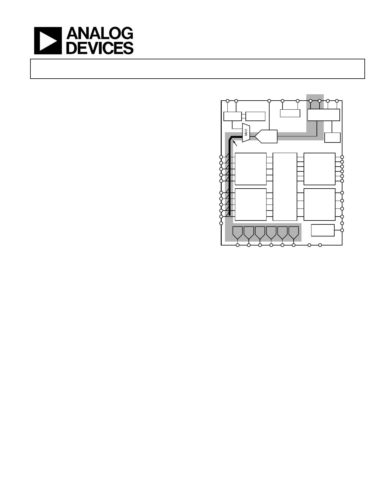
DP DN
DETAILED BLOCK DIAGRAM
REFIN REFOUT
REFGND SDA SCL A1 A0
TEMP
SENSOR
INTERNAL
DIODE
ADM1062
VREF
SMBus
INTERFACE
VX1
VX2
VX3
VX4
VX5
VP1
VP2
VP3
VP4
VH
AGND
VDDCAP
SELECTABLE
ATTENUATOR
SELECTABLE
ATTENUATOR
VDD
ARBITRATOR
12-BIT
SAR ADC
DEVICE
CONTROLLER
OSC
EEPROM
GPI SIGNAL
CONDITIONING
SFD
CONFIGURABLE
OUTPUT DRIVER
(HV)
GPI SIGNAL
CONDITIONING
SFD
SFD
SEQUENCING
ENGINE
CONFIGURABLE
OUTPUT DRIVER
(HV)
CONFIGURABLE
OUTPUT DRIVER
(LV)
SFD
REG 5.25V
CHARGE PUMP
VOUT
DAC
CONFIGURABLE
OUTPUT DRIVER
(LV)
VOUT
DAC
PDO1
PDO2
PDO3
PDO4
PDO5
PDO6
PDO7
PDO8
PDO9
PDO10
PDOGND
GND
VCCP
DAC1 DAC2 DAC3 DAC4 DAC5 DAC6
Figure 2.
Rev. D | Page 4 of 35
5 Page 
ADM1062
Data Sheet
Pin No.
40-Lead 48-Lead
LFCSP
TQFP
37 44
38 45
39 46
Mnemonic
DN
DP
VDDCAP
40 47
GND1
N/A2
EPAD
Description
External Temperature Sensor Cathode Connection.
External Temperature Sensor Anode Connection.
Device Supply Voltage. Linearly regulated from the highest of the VPx, VH pins to a typical of
4.75 V. Note that the capacitor must be connected between this pin and GND. A 10 μF
capacitor is recommended for this purpose.
Supply Ground.
Exposed Pad. The LFCSP has an exposed pad on the bottom. This pad is a no connect (NC). If
possible, this pad should be soldered to the board for improved mechanical stability.
1 In a typical application, all ground pins are connected together.
2 N/A is not applicable
Rev. D | Page 10 of 35
11 Page | ||
| Páginas | Total 30 Páginas | |
| PDF Descargar | [ Datasheet ADM1062.PDF ] | |
Hoja de datos destacado
| Número de pieza | Descripción | Fabricantes |
| ADM1060 | Communications System Supervisory/Sequencing Circuit | Analog Devices |
| ADM1062 | Super Sequencer with Margining Control and Temperature Monitoring | Analog Devices |
| ADM1063 | Multisupply Supervisor/Sequencer | Analog Devices |
| ADM1064 | Super Sequencer with Voltage Readback ADC | Analog Devices |
| Número de pieza | Descripción | Fabricantes |
| SLA6805M | High Voltage 3 phase Motor Driver IC. |
Sanken |
| SDC1742 | 12- and 14-Bit Hybrid Synchro / Resolver-to-Digital Converters. |
Analog Devices |
|
DataSheet.es es una pagina web que funciona como un repositorio de manuales o hoja de datos de muchos de los productos más populares, |
| DataSheet.es | 2020 | Privacy Policy | Contacto | Buscar |