|
|
|
PDF 95HS01 Data sheet ( Hoja de datos )
| Número de pieza | 95HS01 | |
| Descripción | NM95HS01 | |
| Fabricantes | National Semiconductor | |
| Logotipo | ||
Hay una vista previa y un enlace de descarga de 95HS01 (archivo pdf) en la parte inferior de esta página. Total 20 Páginas | ||
|
No Preview Available !
www.DataSheet4U.com
February 1996
NM95HS01 NM95HS02
HiSeCTM High Security Rolling Code Generator
General Description
Features
The NM95HS01 02 HiSeC Rolling Code Generator is a
small footprint monolithic CMOS device designed to pro-
vide a complete low-cost high security solution to the prob-
lem of generating encrypted signals for remote keyless en-
try (RKE) applications
The NM95HS01 02 generates a fully encoded bit stream
each time one of (up to) 4 switch inputs is activated The
patented coding scheme utilizes 248 possible user-pro-
grammable coding combinations and features high linear
complexity and correlation immunity High security is guar-
anteed by generating a unique (rolling) code for each trans-
mission and can be further enhanced by creating custom-
ized algorithms for individual customers With this product
each key can be designed to be both unique and highly
secure
Y High security coding scheme with 248 combinations
Y High linear complexity and correlation immunity
Y 2 2V to 6 5V operation
Y Less than 1 mA standby current
Y Full resynchronization capability
Y Unique customized algorithm option
Y 13 bytes on-chip non-volatile configuration memory
Y RC or XTAL clock options for to 4 1 MHz operation
Y Supports both IR and RF signal transmission
Y Selection of bit coding and transmission frame formats
Y Space saving narrow body SO8 or SO14 packages
Y Up to 4 key switch inputs on SO14 package
Applications
The NM95HS01 02 supports either an IR or RF signal
transmitter and can be clocked with either an RC clock
(NM95HS01) or a crystal oscillator (NM95HS02) The de-
vice operates over a voltage range of 2 2V to 6 5V and
offers a low power standby mode (k1 mA) for battery appli-
cations The product is available in both 8-pin and 14-pin SO
packages with 2 or 4 key switch inputs that can be used for
customer presets such as seat positions and vehicle oper-
ating functions such as car door locking unlocking
Y Remote Keyless Entry (RKE) applications
Y Burglar alarms garage door openers
Y Individualized recognition transmission systems
Y Personalized consumer automotive applications
Relevant Documents
Y MM57HS01 datasheet
Y Designing and Programming a Complete HiSeCTM-
based RKE System
AN-985
Patents Pending
Y HiSeC Remote Keyless Entry Solution Encoder Decod-
DataSheereCth4ipUS.ectoUmser’s Manual
AN-355
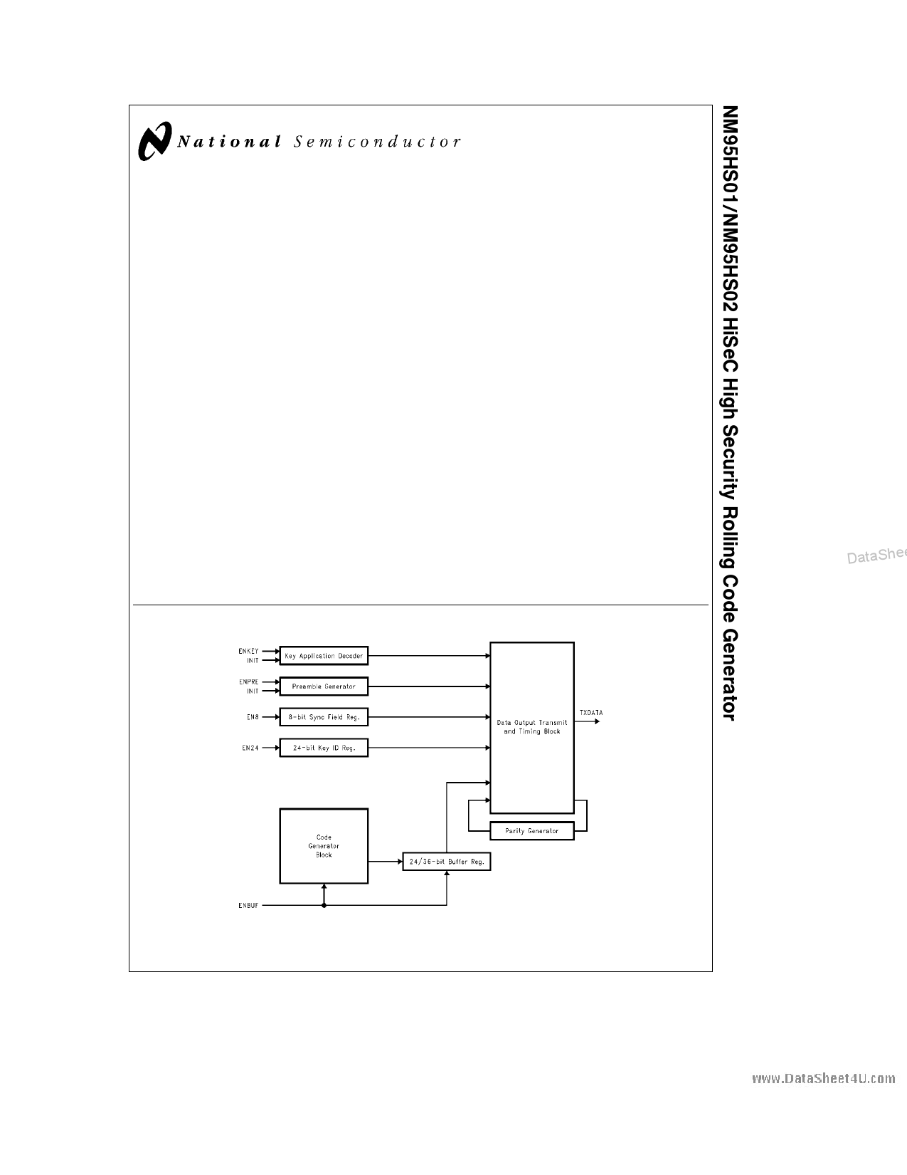
Functional Block Diagram
DataShee
Note Signals shown are internal logic signals
FIGURE 1
HiSeCTM and MICROWIRETM are trademarks of National Semiconductor Corporation
C1996 National Semiconductor Corporation TL D 12302
RRD-B30M66 Printed in U S A
TL D 12302 – 1
DataSheet4U.com
DataSheet4 U .com
1 page 
www.DataSheet4U.com
et4U.com
Bit Coding Formats
The NM95HS01 02 HiSeC Generator supports eleven-bit
coding formats which may be used for IR and RF transmis-
sion Seven-bit formats are available for RF applications
and four are available for IR applications One-bit format is
reserved for future use
Bit coding formats are selected by configuring four bits in
the EEPROM array IRSEL PRSEL2 PRSEL1 and PRSEL0
Table II shows the possible bit coding options available
Each bit coding format has a distinction which may be ad-
vantageous for a particular application RF bit coding format
0 is the simplest bit coding scheme and data may be easily
recovered from a transmission by exclusive OR-ing the data
and clock stream Both RF bit coding formats 0 and 2 have
a DC level that is independent of the data
RF format 4 and the IR modes operate with a constant
transmission energy per message and RF coding formats
1 3 5 and 7 are pulse-width modulated (PWM) formats
which are relatively easy to decode RF coding format 7 has
a low duty cycle
The IR bit coding formats are modulated versions of RF
coding format 4 and are all suitable for IR applications The
duty cycle and number of pulses are variable among these
four to allow the user to fine tune the IR circuit power curve
Bit Transmission Coding Formats
RF Bit Coding Format 0 (Manchester Code)
IR bit coding formats all follow the same general pattern In
this mode a logic ‘‘1’’ is always two periods long and a ‘‘0’’
is always three periods long This may be an important con-
sideration when considering preamble and sync timing
Waveform diagrams for all available RF and IR bit transmis-
sion coding formats are shown below
TABLE II Transmission Bit Coding Options
IRSEL PRSEL2 PRSEL1 PRSEL0
Function
0 0 0 0 RF Bit Coding Format 0
0 0 0 1 RF Bit Coding Format 1
0 0 1 0 RF Bit Coding Format 2
0 0 1 1 RF Bit Coding Format 3
0 1 0 0 RF Bit Coding Format 4
0 1 0 1 RF Bit Coding Format 5
01 1 0
Reserved
0 1 1 1 RF Bit Coding Format 7
1 0 0 0 IR Bit Coding Format 1
1 0 0 1 IR Bit Coding Format 2
1 0 1 0 IR Bit Coding Format 3
1 0 1 1 IR Bit Coding Format 4
11 X X
Reserved
RF Bit Coding Format 1 (33% 66% End High)
DataSheet4U.com
TL D 12302 – 6
RF Bit Coding Format 2 (50% Duty Cycle)
TL D 12302 – 7
RF Bit Coding Format 3 (25% 50% Start High)
DataShee
TL D 12302 – 8
RF Bit Coding Format 4 (IR Style)
TL D 12302 – 9
RF Bit Coding Format 5 (33% 66% Start High)
DataSheet4U.com
DataSheet4 U .com
TL D 12302 – 10
5
TL D 12302 – 11
http www national com
5 Page 
www.DataSheet4U.com
et4U.com
Operational Timing Issues (Continued)
As an example consider the following situation A designer
wishes to design an RF data transmitter using RF bit coding
format 5 with a bit time of 1 ms The designer also wishes to
use a 3 MHz crystal oscillator as the system clock
tor assumes a 6V battery and sets the low battery detect
region to approximately 4 4V to 4 8V If BatteryType e 0
the comparator assumes a 3V battery and sets the low
battery detect region to approximately 2 2V to 2 4V
The required bit time of 1 ms encompasses three RF clock
periods for RF bit coding format 5 Therefore the RF clock
time needs to be of 1 ms (e333 ms) The timer block has
a target value of 2 5 ms (2500 ms) as the output of Prescal-
er3 Since the RF clock signal is divided by Prescaler3 Pre-
scaler3 divides the signal by 2500 333 e 7 5 This figure is
rounded off to become 8
Data output signals are sampled for low voltage at the start
of the data field during frame transmission If a low battery
voltage level is detected and the detect option is enabled
the LED will signal the condition by flashing at the first
pause in the data frame transmission and alternating nor-
mal data field data with a data field containing all ones This
procedure is explained more fully in the Data Field section
One point of possible confusion should be clarified here
Whenever a division value is calculated for any of the 3
prescalers the prescaler should be configured with one unit
less than that division value For example in this case we
calculated a division value of 8 (after rounding) for Prescal-
er3 Therefore Prescaler3 should be programmed with 8 b
1e7
Next we calculate values for Prescaler1 and Prescaler2
Although the crystal oscillator uses both the CKI and CKO
pins only the CKI input is relevant here The CKI input fre-
quency is 3 MHz and of that is 0 75 MHz This is the
input frequency to the HiSeC timer block and the corre-
sponding timing signal is 1 33 ms
Since the RF clock must be 333 ms Prescalers1 and 2 to-
gether must divide by 333 1 33 e 250 A convenient choice
would be to make Prescaler1 divide by 10 and Prescaler2
divide by 25
Therefore load Prescaler1 with 10 b 1 e 9 and Prescal-
er2 with 25 b 1 e 24
Security Aspects
The basis of the HiSeC Generator is to provide a means
of communicating information between the device and its
decoder across some distance Since data is transmitted
at a distance there is a possibility of signal interception
and unauthorized use of the data by a third party The
NM95HS01 02 has been designed to provide such a high
level of complexity and correlation immunity that intercept-
ing the signal is immaterial
INITIALIZATION SYNCHRONIZATION
Initialization is the process of synchronizing the gen-
erator with its decoder for the first time The NM95HS01 02
uses the following procedure to initialize the device
The user inserts a new battery into the HiSeC-based device
which causes the LED to light The LED also has a second-
ary function for synchronization and initialization proce-
dures It will light to prompt the end user that it expects
some action and therefore serves as a guide
DEBOUNCE LOGIC
When the LED lights the user presses a key The LED will
The key switch input signals are connected to the debounce
go off as the generator begins randomizing its registers and
logic block which continuously polls the inputs to determine
configuring its internal logic When the user releases the
if a key switch has been asserted If a key switch hasDbeaetnaSheekte4yUth.ce oLEmD will light a second time This is a signal for the
asserted its normally high input will be seen as a low lf the
user to press a key again This second action shifts the
input is seen low for four continuous debounce strobe sig-
generator into sync mode This causes the NM95HS01 02
nals it is considered to be a stable signal and its associat-
to transmit at least four sync frames allowing the decoder
ed output from the debounce logic block is set high This
to synchronize to the generator The generator then exits
enables the generator control logic and a code is generat-
sync mode and is ready tor normal operation
ed and transmitted
RESYNCHRONIZATION
This debounced output signal is deasserted as soon as the
key is released and its signal goes high again This assumes
normal operation However if a key remained pressed for a
long time the generator might time-out before seeing the
signal go high again (if TIMEOUTEN e 1) The generator
would then enter halt mode even if the key remained
pressed The generator would come out of halt mode when
it saw the falling edge of another key input which would
occur when another key is pressed
LOW BATTERY DETECT OPTION
If synchronization is lost between the generator and its de-
coder resynchronization is accomplished using a sync
frame A sync frame is generated in two cases when the
battery is removed and replaced or the user initiates an
initialization procedure by holding Key Switch 1 and Key
Switch 2 simultaneously for 5 seconds
A sync frame provides the decoder with enough information
to ‘‘learn’’ the key and synchronize to it
For the highest possible security protection resynchroniza-
tion can be completely excluded by configuring the decoder
The NM95HS01 02 contains an internal comparator circuit
to recognize and refuse to act upon the transmission of a
that detects low battery voltage and indicates this condition
sync frame The sync frame format is discussed more fully
to the data frame generator The CompareEnable parame-
elsewhere but briefly it can be recognized by the presence
ter in EEPROM enables this function (CompareEnable e
of all zeroes in the data field In this case if synchronization
1) During halt mode the comparator is switched off com-
is lost between the generator and decoder they could not
pletely to minimize power consumption The BatteryType
be made to function together
parameter in EEPROM selects the threshold voltage range
for the comparator If BatteryType e 1 the compara-
11 http www national com
DataSheet4U.com
DataSheet4 U .com
DataShee
11 Page | ||
| Páginas | Total 20 Páginas | |
| PDF Descargar | [ Datasheet 95HS01.PDF ] | |
Hoja de datos destacado
| Número de pieza | Descripción | Fabricantes |
| 95HS01 | NM95HS01 | National Semiconductor |
| Número de pieza | Descripción | Fabricantes |
| SLA6805M | High Voltage 3 phase Motor Driver IC. |
Sanken |
| SDC1742 | 12- and 14-Bit Hybrid Synchro / Resolver-to-Digital Converters. |
Analog Devices |
|
DataSheet.es es una pagina web que funciona como un repositorio de manuales o hoja de datos de muchos de los productos más populares, |
| DataSheet.es | 2020 | Privacy Policy | Contacto | Buscar |