|
|
PDF HN29V25611AT-50H Data sheet ( Hoja de datos )
| Número de pieza | HN29V25611AT-50H | |
| Descripción | 256M AND Type Flash Memory | |
| Fabricantes | Hitachi | |
| Logotipo |  |
|
Hay una vista previa y un enlace de descarga de HN29V25611AT-50H (archivo pdf) en la parte inferior de esta página. Total 30 Páginas | ||
|
No Preview Available !
www.DataSheet4U.com
HN29V25611AT-50H
256M AND type Flash Memory
More than 16,057-sector (271,299,072-bit)
ADE-203-1334A (Z)
Rev. 1.0
Apr. 5, 2002
Description
The Hitachi HN29V25611AT-50H Series is a CMOS Flash Memory with AND type multi-level memory
cells. It has fully automatic programming and erase capabilities with a single 3.0 V power supply. The
functions are controlled by simple external commands. To fit the I/O card applications, the unit of
programming and erase is as small as (2048 + 64) bytes. Initial available sectors of HN29V25611AT-50H are
more than 16,057 (98% of all sector address) and less than 16,384 sectors.
Features
• On-board single power supply (VCC): VCC = 2.7 V to 3.6 V
• Organization
AND Flash Memory: (2048 + 64) bytes × (More than 16,057 sectors)
Data register: (2048 + 64) bytes
• Multi-level memory cell
2 bit/per memory cell
• Automatic programming
Sector program time: 1.0 ms (typ)
System bus free
Address, data latch function
Internal automatic program verify function
Status data polling function
• Automatic erase
Single sector erase time: 1.0 ms (typ)
System bus free
Internal automatic erase verify function
Status data polling function
www.DataSheet4U.com
1 page 
www.DataSheet4U.com
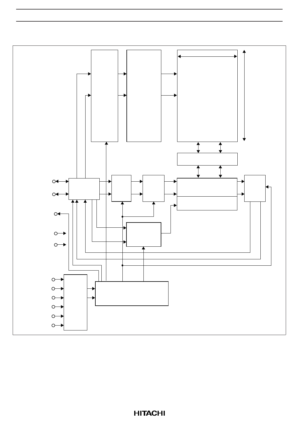
Block Diagram
HN29V25611AT-50H
Sector
address
buffer
X-decoder
2048 + 64
16384 × (2048 + 64) × 8
memory matrix
Data register (2048 + 64)
••
I/O0
to
I/O7
••
• Multiplexer •
Data •
input
buffer
•
Input •
data
control
•
RDY/Busy
••
Y-gating
Y-decoder
Data
output
buffer
•••
VCC
VSS
• Y-address
• counter
CE
OE
WE
SC
RES
CDE
Control
signal
buffer
Read/Program/Erase control
www.DataSheet4U.com
5
5 Page 
HN29V25611AT-50Hwww.DataSheet4U.com
Mode Description
Read
Serial Read (1): Memory data D0 to D2111 in the sector of address SA is sequentially read. Output data is
not valid after the number of the SC pulse exceeds 2112. When CA is input, memory data D (m) to D (m + j)
in the sector of address SA is sequentially read. Then output data is not valid after the number of the SC pulse
exceeds (2112 to m). The mode turns back to the standby mode at any time when CE is VIH.
Serial Read (2): Memory data D2048 to D2111 in the sector of address SA is sequentially read. Output data
is not valid after the number of the SC pulse exceeds 64. The mode turns back to the standby mode at any
time when CE is VIH.
Automatic Erase
Single Sector Erase: Memory data D0 to D2111 in the sector of address SA is erased automatically by
internal control circuits. After the sector erase starts, the erasure completion can be checked through the
RDY/Busy signal and status data polling. All the bits in the sector are "1" after the erase. The sector valid
data stored in a part of memory data D2048 to D2111 must be read and kept outside of the sector before the
sector erase.
Automatic Program
Program (1): Program data PD0 to PD2111 is programmed into the sector of address SA automatically by
internal control circuits. When CA is input, program data PD (m) to PD (m + j) is programmed from CA into
the sector of address SA automatically by internal control circuits. By using program (1), data can
additionally be programed 15 times for each sector before the following erase. When the column is
programmed, the data of the column must be [FF]. After the programming starts, the program completion can
be checked through the RDY/Busy signal and status data polling. Programmed bits in the sector turn from
"1" to "0" when they are programmed. The sector valid data should be included in the program data PD2048
to PD2111.
Program (2): Program data PD0 to PD2111 is programmed into the sector of address SA automatically by
internal control circuits. After the programming starts, the program completion can be checked through the
RDY/Busy signal and status data polling. Programmed bits in the sector turn from "1" to "0" when they are
programmed. The sector must be erased before programming. The sector valid data should be included in the
program data PD2048 to PD2111.
Program (3): Program data PD2048 to PD2111 is programmed into the sector of address SA automatically
by internal control circuits. By using program (3), data can additionally be programed 15 times for each
sector befor the following erase. When the column is programmed, the data of the column must be [FF].
After the programming starts, the program completion can be checked through the RDY/Busy signal and
status data polling. Programmed bits in the sector turn from "1" to "0" when they are programmed.
www.DataSheet4U.com
11
11 Page | ||
| Páginas | Total 30 Páginas | |
| PDF Descargar | [ Datasheet HN29V25611AT-50H.PDF ] | |
Hoja de datos destacado
| Número de pieza | Descripción | Fabricantes |
| HN29V25611AT-50H | 256M AND Type Flash Memory | Hitachi |
| Número de pieza | Descripción | Fabricantes |
| SLA6805M | High Voltage 3 phase Motor Driver IC. |
Sanken |
| SDC1742 | 12- and 14-Bit Hybrid Synchro / Resolver-to-Digital Converters. |
Analog Devices |
|
DataSheet.es es una pagina web que funciona como un repositorio de manuales o hoja de datos de muchos de los productos más populares, |
| DataSheet.es | 2020 | Privacy Policy | Contacto | Buscar |
