|
|
|
PDF ADD8502 Data sheet ( Hoja de datos )
| Número de pieza | ADD8502 | |
| Descripción | Integrated LCD Grayscale Generator | |
| Fabricantes | Analog Devices | |
| Logotipo | ||
Hay una vista previa y un enlace de descarga de ADD8502 (archivo pdf) en la parte inferior de esta página. Total 16 Páginas | ||
|
No Preview Available !
a
Integrated LCD
Grayscale Generator
ADD8502
FEATURES
Two Mask Programmable Sets of Five Reference Levels
Dual 10-Bit DACs for Flicker Offset and Range Adjustment
Integrated VCOM Switching
Single-Supply Operation: 5.0 V
Low Supply Current: 300 A
Global Power Save Mode: 1 A Max
Fast Settling Time for Load Change: 20 s
Stable with 20 nF/100 ⍀ Loads
CMOS/TTL Input Levels
APPLICATIONS
Color TFT Cell Phones
Color TFT PDAs
GENERAL DESCRIPTION
The ADD8502 is an integrated, high accuracy, programmable
grayscale generator. Two sets of five output reference voltages
are mask programmed to 0.2% resolution. The outputs switch
between the two sets of five levels. The reference levels are selected
from a 512 tap resistor network using a via mask.
ADD8502 includes two serially addressable, 10-bit digital-to-
analog converters (DACs) and five fast, low current buffers.
The dual DACs set the endpoint voltages applied to the resistor
network to adjust for flicker and range. The two power save modes
can reduce the total current to less than 1 µA and feature fast
recovery time from Shutdown/Sleep Mode. The ADD8502
accepts CMOS or TTL inputs for all controls, including the
common drive circuit levels.
ADD8502 operates over the industrial temperature range from
–40°C to +85°C and is available in a space-saving 24-lead
4 mm ϫ 4 mm frame chip scale package.
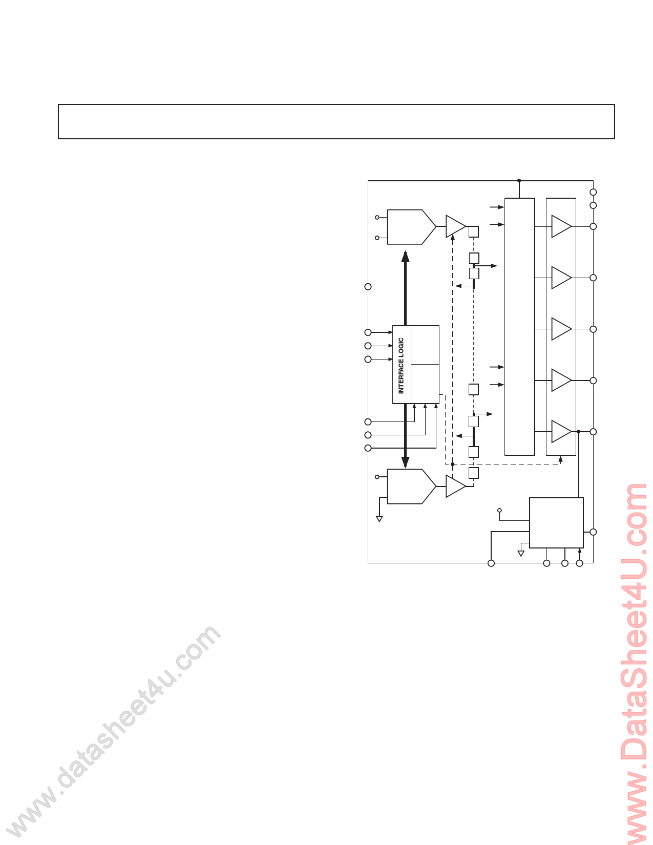
FUNCTIONAL BLOCK DIAGRAM
REV2
VDD
VREF+
VDD/2
10-BIT
DAC A
VREF–
VL
VP0
VN0
R
R VP0
R
VN4
A0
A1
SCK
DIN
CS-LD
DIGITAL
CORE
POWER
SAVE
LOGIC
PSK
GS1
GS2
VDD/2
VREF+
10-BIT
DAC B
VREF–
MUX
VP4
VN4
R
VP4
R
VN0
R
R
VDD
A2
A3
A4
VCOM
LOGIC
VDD
GND
V0
V1
V2
V3
V4
COM
COM_M
REV1 CM CV4
sheet4u.comREV. 0
taInformation furnished by Analog Devices is believed to be accurate and
areliable. However, no responsibility is assumed by Analog Devices for its
.duse, nor for any infringements of patents or other rights of third parties
that may result from its use. No license is granted by implication or
wwwotherwise under any patent or patent rights of Analog Devices.
One Technology Way, P.O. Box 9106, Norwood, MA 02062-9106, U.S.A.
Tel: 781/329-4700
www.analog.com
Fax: 781/326-8703
© Analog Devices, Inc., 2002
1 page 
PIN CONFIGURATION
ADD8502
24 23 22 21 20 19
VL 1
DIN 2
SCK 3
CS-LD 4
CM 5
CV4 6
PIN 1
IDENTIFIER
ADD8502
TOP VIEW
(Not to Scale)
18 V0
17 V1
16 V2
15 V3
14 V4
13 GND
7 8 9 10 11 12
NC = NO CONNECT
PIN FUNCTION DESCRIPTIONS
Pin No. Mnemonic Name
I/O Description
1 VL
2 DIN
Logic Select Pin I
Serial Data Input I
Logic Supply Voltage. Connect to supply used for system logic. Can accept 2.7 V to VDD.
When CS is LOW, the input on this pin is shifted into the internal shift register on
the rising edge of SCK.
3
SCK
Serial Clock
I Accepts up to 10 MHz input. The rising edge on this clock will shift the data on
4 CS-LD Load
DIN Pin into the internal shift registers.
I When CS-LD is LOW, SCK is enabled for shifting data on the DIN input into the
internal shift register on the rising edge of SCK. Data is loaded MSB first.
5 CM Logic Control 2 I When CM is LOW, COM will output the voltage level input on COM_M.
for VCOM
When CM is HIGH, COM levels will be determined by the input on REV1.
6 CV4 Logic Control V4 I If CV4 is HIGH, V4 output is the output of the op amp A4. If CV4 is LOW, V4 is
connected to COM and op amp A4 is shut down. Refer to Table II.
7
REV1
Logic Control 1 I With CM HIGH, a HIGH on REV1 will cause COM to output the voltage level
for VCOM
input at VDD. A LOW on REV1 will cause COM to output the voltage level input
at GND.
8 NC
No Connect
Unused Pin
9 NC
No Connect
Unused Pin
10 COM Common Output O If CM is LOW, COM will output the voltage input at COM_M. If CM is HIGH,
COM will output the voltage input at VDD when REV1 is HIGH and will output
the voltage input at GND when REV1 is LOW. Refer to Table II.
11 COM_M Common System I COM_M is a system voltage reference input between 2.5 V and 3.5 V. This may
12 NC
VREF
No Connect
be the system 3.3 V supply.
Unused Pin
13 GND Ground
I Ground. Nominally 0 V.
14 V4
Output
O Buffers are rail-to-rail buffers that can drive high capacitive loads (>16.5 nF).
When PSK is LOW, these outputs will be Hi-Z.
15 V3
Output
O Buffers are rail-to-rail buffers that can drive high capacitive loads (>16.5 nF).
When PSK is LOW or GS1 and GS2 = HIGH, these outputs will be Hi-Z.
16 V2
Output
O Buffers are rail-to-rail buffers that can drive high capacitive loads (>16.5 nF).
When PSK is LOW or GS1 and GS2 = HIGH, these outputs will be Hi-Z.
17 V1
Output
O Buffers are rail-to-rail buffers that can drive high capacitive loads (>16.5 nF).
When PSK is LOW or GS1 and GS2 = HIGH, these outputs will be Hi-Z.
18 V0
Output
O Buffers are rail-to-rail buffers that can drive high capacitive loads (>16.5 nF).
When PSK is LOW, these outputs will be Hi-Z.
19 VDD
20 NC
Supply
No Connect
I Supply Voltage. Nominally 5 V.
Unused Pin
REV. 0
–5–
5 Page 
ADD8502
OPERATION
Transfer Function
The transfer function for the ADD8502 is given in the following
equations:
1. Digital-to-analog transfer function for DAC A. An output can
be derived from Equation 1 as:
VOUTA
=
VDD
2
1
+
DA
1024
(1)
2. Digital-to-analog transfer function for DAC B. An output can
be derived from Equation 2 as:
VOUTB
=
DB
1024
VDD
2
(2)
Where DA and DB are decimal equivalents of the binary codes
that are loaded to the DAC Register from 0 to 1023.
3. Using any programmed tap point from the 512 resistor string,
the system output can be derived from Equation 3:
VTX
= (VOUTA
−
VOUTB
)
TX
512
+
VOUTB
(3)
Where TX is any tap point of the 512 resistor string. It is mask
programmable. VTX is the voltage output at any output (VO, ... V4)
and will switch between two voltages depending on the mask
programmed tap points.
Example: VDD = 5 V, DA = 1,000, DB = 100, and TX = 500.
VOUTA = 4.941 V
VOUTB = 0.244 V
VTX = 4.831 V
Equations 1–3 will provide a theoretical calculation of the out-
puts. The actual will vary with load, process, and architecture.
See Specifications table.
SERIAL INTERFACE
The ADD8502 has a 3-wire serial interface (CS-LD, SCK, and
DIN). The writing sequence begins by bringing the CS-LD line
LOW. Data on the DIN line is clocked into the 16-bit shift regis-
ter on the rising edge of SCK. The serial clock frequency can be
as high as 10 MHz. When the last data bit is clocked in,
CS-LD line needs to be brought HIGH to load the DAC regis-
ters and the operation mode is dependent upon the control bits.
Input Shift Register
The input shift register is 16 bits wide (see Figure 4). The first
four control bits (C3, C2, C1, and C0) are used to set the different
operating modes of the device. The next 10 bits are the data bits
and the last two bits are “Don’t Cares.” This composes a full word
that is transferred to the DAC register on the rising edge of CS-LD.
In a normal write sequence, the CS-LD line is kept LOW for at
least 16 rising edges of SCK and then it is brought HIGH to
update the DACs. However, if CS-LD is brought HIGH before
the 16th rising edge, this acts as an interrupt to the write sequence.
The shift register is reset and the write sequence is seen as invalid.
Neither an update of the DAC register contents nor a change in
the operation mode occurs.
DB15 (MSB)
DB0 (LSB)
C3 C2 C1 C0 D9 D8 D7 D6 D5 D4 D3 D2 D1 D0 X1 X0
CONTROL BITS
DATA BITS
Figure 4. Input Register Contents
DON’T
CARE
REV. 0
–11–
11 Page | ||
| Páginas | Total 16 Páginas | |
| PDF Descargar | [ Datasheet ADD8502.PDF ] | |
Hoja de datos destacado
| Número de pieza | Descripción | Fabricantes |
| ADD8502 | Integrated LCD Grayscale Generator | Analog Devices |
| ADD8502 | Integrated LCD Grayscale Generator | Analog Devices |
| ADD8504 | (ADD8504 - ADD8506) Muxed Input Line Inversion LCD Gamma Buffers | Analog Devices |
| ADD8505 | (ADD8504 - ADD8506) Muxed Input Line Inversion LCD Gamma Buffers | Analog Devices |
| Número de pieza | Descripción | Fabricantes |
| SLA6805M | High Voltage 3 phase Motor Driver IC. |
Sanken |
| SDC1742 | 12- and 14-Bit Hybrid Synchro / Resolver-to-Digital Converters. |
Analog Devices |
|
DataSheet.es es una pagina web que funciona como un repositorio de manuales o hoja de datos de muchos de los productos más populares, |
| DataSheet.es | 2020 | Privacy Policy | Contacto | Buscar |