|
|
|
PDF C5001 Data sheet ( Hoja de datos )
| Número de pieza | C5001 | |
| Descripción | Low Skew Muliple Frequency PCI Clock Generator with EMI Reducing SSCG | |
| Fabricantes | International | |
| Logotipo | ||
Hay una vista previa y un enlace de descarga de C5001 (archivo pdf) en la parte inferior de esta página. Total 13 Páginas | ||
|
No Preview Available !
C5001
Low Skew Multiple Frequency PCI Clock Generator with EMI Reducing SSCG.
Approved Product
Product Features
S Produces PCI output clocks that are individually
selectable for 33.3 or 66.6 MHz under I2C or
strapping control.
S Separate output buffer power supply for reduced
noise, crosstalk and jitter.
S input clock frequency standard 14.31818 MHz
S Output clocks frequency individually selectable via
I2C or hardware bi-directional pin strapping.
S SSCG EMI reduction at 1.0% width
S Individual clock disables via I2C control
S All output clocks skewed within a 500 pS window
S Cycle to Cycle jitter ± 250 pS
S Output duty cycle is automatically 50% (±10%)
adjusted
S Clock feed through mode and OE pins for logic
testing
S Glitchless clock enabling and disabling transitions
S 28-pin TSSOP or SSOP package
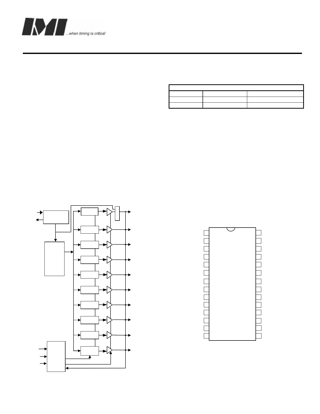
Block Diagram
XIN
XOUT
Reference
Oscillator
÷1 ÷2
÷1 ÷2
M
U REF-
X CLK0/S0
CLK1/S1
PLL
÷1 ÷2
÷1 ÷2
CLK2/S2
CLK3/S3
÷1 ÷2
CLK4/S4
÷1 ÷2
CLK5/S5
÷1 ÷2
CLK6/S6
÷1 ÷2
CLK7/S7
÷1 ÷2
CLK8/S8
Output Enable logic Functionality Table
OE CLK(0:9)
PLL
1 (HIGH)
Enabled
Running
0 (LOW)
Tri State
Running
Pin Configuration
VDD
XIN
XOUT
VSS
OE
SCLK
SDATA
VSS
VSS
CLK9/S9
CLK8/S8
VDD5
VSS
CLK7/S7
1
2
3
4
5
6
7
8
9
10
11
12
13
14
28 VDD1
27 REF-CLK0/S0
26 CLK1/S1
25 VSS
24 VDD2
23 CLK2/S2
22 CLK3/S3
21 VSS
20 VDD3
19 CLK4/S4
18 CLK5/S5
17 VSS
16. VDD4
15 CLK6/S6
OE
SDATA
SCLK
I2C
LOGIC
÷1 ÷2
÷4, ÷8
CLK9/S9
INTERNATIONAL MICROCIRCUITS, INC. 525 LOS COCHES ST.
MILPITAS, CA 95035. TEL: 408-263-6300. FAX 408-263-6571
Rev. 2.1
6/14/1999
Page 1 of 13
1 page 
C5001
Low Skew Multiple Frequency PCI Clock Generator with EMI Reducing SSCG.
Approved Product
Application Note for Selection on Bi-Directional Pins
Pins 10, 11, 14, 15, 18, 19, 22, 23, 26 and 27 are Power
up bi-directional pins and are used for selecting power
up output frequencies of this devices output clocks (see
Pin description, Page 2). During power-up of the device,
these pins are in input mode, therefore, they are
considered input select pins internal to the IC, these
pins have a large value pull-up each (250KΩ), therefore,
a selection “1” is the default and will select a 66 MHz
output frequency. If the system uses a slow power
supply (over 5 ms settling time), then it is recommended
to use an external pull-up (Rup) in order to insure a high
selection. In this case, the designer may choose one of
two configurations, see FIG. 3A and Fig. 3B.
Fig. 3A represents an additional pull up resistor 50KΩ
connected from the pin to the power line, which allows a
faster pull to a high level.
If a selection “0” is desired, then a jumper is placed on
JP1 to a 5KΩ resistor as implemented as shown in Fig.
3A. Please note the selection resistors (Rup and Rdn)
are placed before the Damping resistor (Rd) close to
the pin.
C5001
Bidirectional
Vdd
Rup
50K
Rd
Load
JP1
JUMPER
Rdn
5K
Fig.3A
Vdd JP2
3 Way Jumper
Fig. 3B represents a single resistor 10KΩ connected to
a 3-way jumper, JP2. When a “1” selection is desired, a
jumper is placed between leads 1 and 3. When a “0”
selection is desired, a jumper is placed between leads 1
and 2.
C5001
Bidirectional
Rsel
10K
Rd
Load
If the system power supply is fast (less than 5 mSec
settling time), then Fig. 3A only applies and Pull up Rup
resistor is not necessary.
Fig.3B
The electrical length of the trace that connects the
selection resistor to the devices pin should be kept as
short as possible.
Input and Output Relationships
The device acts a PCI clock generator. Output clocks may be individually controlled to be either 33.3 or 66.6 MHz in
frequency by setting or clearing the clocks respective I2C control register bit. All output clocks are rising edge aligned to
within a shared 500 pS window. There is no specified relationship between the input reference clock and the output
clocks.
INTERNATIONAL MICROCIRCUITS, INC. 525 LOS COCHES ST.
MILPITAS, CA 95035. TEL: 408-263-6300. FAX 408-263-6571
Rev.2.1
6/14/1999
Page 5 of 13
5 Page 
C5001
Low Skew Multiple Frequency PCI Clock Generator with EMI Reducing SSCG.
Approved Product
Package Drawing and Dimensions
D
B
EH
C
L
A2
A1
e
a
A
28 Pin SSOP Outline Dimensions
INCHES
MILLIMETERS
SYMBOL MIN
NOM MAX MIN NOM MAX
A 0.068 0.073 0.078 1.73 1.86 1.99
A1 0.002 0.005 0.008 0.05 0.13 0.21
A2 0.066 0.068 0.070 1.68 1.73 1.78
B 0.010 0.012 0.015 0.25 0.30 0.38
C 0.005 0.006 0.009 0.13 0.15 0.22
D 0.397 0.402 0.407 10.07 10.20 10.33
E 0.205 0.209 0.212 5.20 5.30 5.38
e 0.0256 BSC
0.65 BSC
H 0.301` 0.307 0.311 7.65 7.80 7.90
a 0° 4° 8° 0° 4° 8°
L 0.022 0.030 0.037 0.55 0.75 0.95
INTERNATIONAL MICROCIRCUITS, INC. 525 LOS COCHES ST.
MILPITAS, CA 95035. TEL: 408-263-6300. FAX 408-263-6571
Rev.2.1
6/14/1999
Page 11 of 13
11 Page | ||
| Páginas | Total 13 Páginas | |
| PDF Descargar | [ Datasheet C5001.PDF ] | |
Hoja de datos destacado
| Número de pieza | Descripción | Fabricantes |
| C5000 | NPN Transistor - 2SC5000 | Toshiba Semiconductor |
| C5001 | Low Skew Muliple Frequency PCI Clock Generator with EMI Reducing SSCG | International |
| C5002 | Low Skew Muliple Frequency PCI Clock Generator with EMI Reducing SSCG | International |
| C5002 | NPN Transistor - 2SC5002 | Sanken electric |
| Número de pieza | Descripción | Fabricantes |
| SLA6805M | High Voltage 3 phase Motor Driver IC. |
Sanken |
| SDC1742 | 12- and 14-Bit Hybrid Synchro / Resolver-to-Digital Converters. |
Analog Devices |
|
DataSheet.es es una pagina web que funciona como un repositorio de manuales o hoja de datos de muchos de los productos más populares, |
| DataSheet.es | 2020 | Privacy Policy | Contacto | Buscar |