|
|
|
PDF WM8191 Data sheet ( Hoja de datos )
| Número de pieza | WM8191 | |
| Descripción | 14-bit 6MSPS CIS/CCD Analogue Front End/Digitiser | |
| Fabricantes | Wolfson Microelectronics plc | |
| Logotipo | ||
Hay una vista previa y un enlace de descarga de WM8191 (archivo pdf) en la parte inferior de esta página. Total 27 Páginas | ||
|
No Preview Available !
WM8191
14-bit 6MSPS CIS/CCD Analogue Front End/Digitiser
Advanced Information, April 2001, Rev 3.1
DESCRIPTION
The WM8191 is a 14-bit analogue front end/digitiser IC
which processes and digitises the analogue output signals
from CCD sensors or Contact Image Sensors (CIS) at pixel
sample rates of up to 6MSPS.
The device includes three analogue signal processing
channels each of which contains Reset Level Clamping,
Correlated Double Sampling and Programmable Gain and
Offset adjust functions. Three multiplexers allow single
channel processing. The output from each of these
channels is time multiplexed into a single high-speed 14-bit
analogue-to-digital converter. The digital output data is
available in 14-bit parallel or 8/7/4-bit wide multiplexed
format, with no missing codes.
An internal 4-bit DAC is supplied for internal reference level
generation. This may be used during CDS to reference CIS
signals or during Reset Level Clamping to clamp CCD
signals. Alternatively an external reference level may be
applied. ADC references are generated internally, ensuring
optimum performance from the device.
Using an analogue supply voltage of 5V and a digital
interface supply of either 5V or 3.3V, the WM8191 typically
only consumes 250mW when operating from a single 5V
supply and less than 1µA when in power down mode.
FEATURES
• 14-bit ADC
• No missing codes guaranteed
• 6MSPS conversion rate
• Low power – 250mW typical
• 5V single supply or 5V/3.3V dual supply operation
• Single or 3 channel operation
• Correlated double sampling
• Programmable gain (8-bit resolution)
• Programmable offset adjust (8-bit resolution)
• Programmable clamp voltage
• 14-bit parallel or 8/7/4-bit wide multiplexed data output
formats
• Internally generated voltage references
• 48-pin TQFP package
• Serial or parallel control interface
APPLICATIONS
• Flatbed and sheetfeed scanners
• USB compatible scanners
• Multi-function peripherals
• High-performance CCD sensor interface
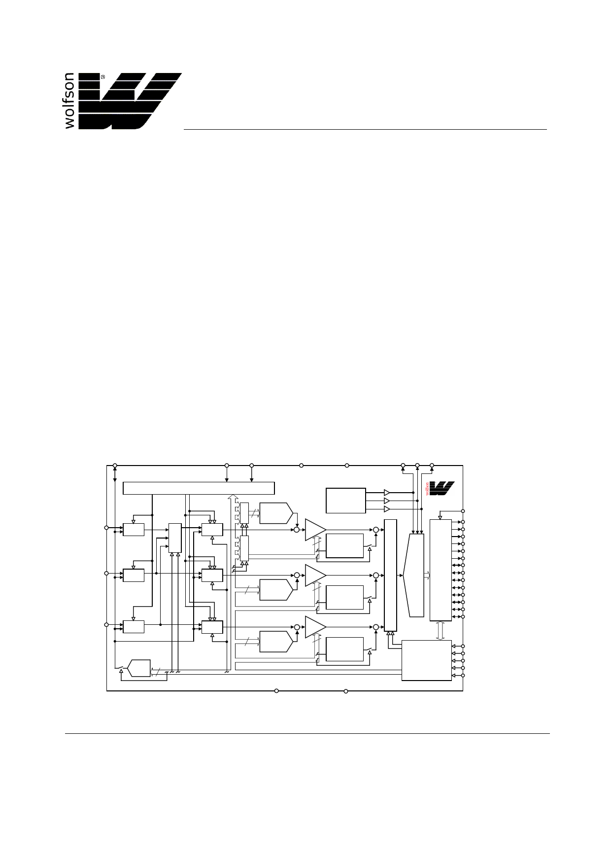
BLOCK DIAGRAM
VRLC/VBIAS
(2)
VSMP MCLK
(15) (17)
AVDD1-2
(43, 44)
DVDD1-3
(10, 24, 35)
VRT VRX VRB
(48) (1) (47)
RINP (8)
GINP (6)
BINP (4)
CL
RLC
RLC
RLC
RLC 4
DAC
RS VS
M
U
X
TIMING CONTROL
CDS
RM
GU
X
B
8
OFFSET
DAC
+ PGA
RM
GU
X
B
8
VREF/BIAS
I/P SIGNAL
POLARITY
ADJUST
CDS
+ PGA
8 OFFSET
DAC
8 I/P SIGNAL
POLARITY
ADJUST
CDS
+ PGA
8 OFFSET
DAC
8 I/P SIGNAL
POLARITY
ADJUST
WM8191
+
M
+U
X
14-
BIT
ADC
DATA
I/O
PORT
+
CONFIGURABLE
SERIAL/
PARALLEL
CONTROL
INTERFACE
(11) OEB
(21) OP[0]
(22) OP[1]
(23) OP[2]
(26) OP[3]
(27) OP[4]
(28) OP[5]
(29) OP[6]
(31) OP[7]
(32) OP[8]
(33) OP[9]
(34) OP[10]
(37) OP[11]
(38) OP[12]
(39) OP[13]/SDO
(12) SEN/STB
(14) SCK/RNW
(13) SDI/DNA
(16) RLC/ACYC
(42) NRESET
(3, 5, 7, 9, 45, 46)
AGND1-6
(18, 25, 30, 36, 40)
DGND1-5
WOLFSON MICROELECTRONICS LTD
Lutton Court, Bernard Terrace, Edinburgh, EH8 9NX, UK
Tel: +44 (0) 131 667 9386
Fax: +44 (0) 131 667 5176
Email: [email protected]
www.wolfsonmicro.com
Advanced Information data sheets contain
preliminary data on new products in the
preproduction phase of development.
Supplementary data will be published at a
later date.
2001 Wolfson Microelectronics Ltd.
1 page 
Advanced Information
WM8191
ELECTRICAL CHARACTERISTICS
Test Conditions
AVDD1 = AVDD2 = DVDD1 =4.75 to 5.25V, DVDD2 = DVDD3 = 2.97 to 3.63V, AGND = DGND = 0V, TA = 0 to 70°C, MCLK =
12MHz unless otherwise stated.
PARAMETER
SYMBOL
TEST
CONDITIONS
MIN TYP MAX
Overall System Specification (including 14-bit ADC, PGA, Offset and CDS functions)
NO MISSING CODES GUARANTEED
Full-scale input voltage range
Max Gain
0.4
(see Note 1)
Min Gain
4.08
Input signal limits (see Note 2)
VIN
0 AVDD
Full-scale transition error
Gain = 0dB;
20
PGA[7:0] = 4B(hex)
Zero-scale transition error
Gain = 0dB;
PGA[7:0] = 4B(hex)
20
Differential non-linearity
DNL
0.65
Integral non-linearity
INL
4
Channel to channel gain matching
1
References
Upper reference voltage
VRT
2.85
Lower reference voltage
VRB
1.35
Input return bias voltage
VRX
0.65
Diff. reference voltage (VRT-VRB)
Output resistance VRT, VRB, VRX
VRTB
1.4 1.5 1.6
1
VRLC/Reset-Level Clamp (RLC)
RLC switching impedance
50
VRLC short-circuit current
5
VRLC output resistance
2
VRLC Hi-Z leakage current
VRLC = 0 to AVDD
1
RLCDAC resolution
4
RLCDAC step size, RLCDAC = 0
RLCDAC step size, RLCDAC = 1
RLCDAC output voltage at
code 0(hex), RLCDACRNG = 0
VRLCSTEP
VRLCSTEP
VRLCBOT
0.25
0.17
0.41
RLCDAC output voltage at
code 0(hex), RLCDACRNG = 1
VRLCBOT
0.28
RLCDAC output voltage at
code F(hex) RLCDACRNG, = 0
VRLCTOP
4.17
RLCDAC output voltage at
code F(hex), RLCDACRNG = 1
VRLCTOP
2.82
VRLC deviation
-50 +50
Offset DAC, Monotonicity Guaranteed
Resolution
8
Differential non-linearity
DNL
0.1 0.5
Integral non-linearity
INL
0.25 1
Step size
2.04
Output voltage
Code 00(hex)
-260
Code FF(hex)
+260
Notes: 1. Full-scale input voltage denotes the maximum amplitude of the input signal at the specified gain.
2. Input signal limits are the limits within which the full-scale input voltage signal must lie.
UNIT
Vp-p
Vp-p
V
mV
mV
LSB
LSB
%
V
V
V
V
Ω
Ω
mA
Ω
µA
bits
V/step
V/step
V
V
V
V
mV
bits
LSB
LSB
mV/step
mV
mV
WOLFSON MICROELECTRONICS LTD
AI Rev 3.1 April 2001
5
5 Page 
Advanced Information
WM8191
DEVICE DESCRIPTION
INTRODUCTION
A block diagram of the device showing the signal path is presented on Page 1.
The WM8191 samples up to three inputs (RINP, GINP and BINP) simultaneously. The device then
processes the sampled video signal with respect to the video reset level or an internally/externally
generated reference level using either one or three processing channels.
Each processing channel consists of an Input Sampling block with optional Reset Level Clamping
(RLC) and Correlated Double Sampling (CDS), a 8-bit programmable offset DAC and an 8-bit
Programmable Gain Amplifier (PGA).
The ADC then converts each resulting analogue signal to a 14-bit digital word. The digital output from
the ADC is presented on a 14-bit wide bus, with optional 8+6-bit, 7+7-bit or 4+4+4+2-bit multiplexed
formats.
On-chip control registers determine the configuration of the device, including the offsets and gains
applied to each channel. These registers are programmable via a serial or parallel interface.
INPUT SAMPLING
The WM8191 can sample and process one to three inputs through one or three processing channels
as follows:
Colour Pixel-by-Pixel: The three inputs (RINP, GINP and BINP) are simultaneously sampled for
each pixel and a separate channel processes each input. The signals are then multiplexed into the
ADC, which converts all three inputs within the pixel period.
Monochrome: A single chosen input (RINP, GINP, or BINP) is sampled, processed by the
corresponding channel, and converted by the ADC. The choice of input and channel can be changed
via the control interface, e.g. on a line-by-line basis if required.
Colour Line-by-Line: A single chosen input (RINP, GINP, or BINP) is sampled and multiplexed into
the red channel for processing before being converted by the ADC. The input selected can be
switched in turn (RINP → GINP → BINP → RINP…) together with the PGA and offset DAC control
registers by pulsing the RLC/ACYC pin. This is known as auto-cycling. Alternatively, other sampling
sequences can be generated via the control registers. This mode causes the blue and green
channels to be powered down. Refer to the Line-by-Line Operation section for more details.
RESET LEVEL CLAMPING (RLC)
To ensure that the signal applied to the WM8191 lies within its input range (0V to AVDD) the CCD
output signal is usually level shifted by coupling through a capacitor, CIN. The RLC circuit clamps the
WM8191 side of this capacitor to a suitable voltage during the CCD reset period.
A typical input configuration is shown in Figure 8 A clamp pulse, CL, is generated from MCLK and
VSMP by the Timing Control Block. When CL is active the voltage on the WM8191 side of CIN, at
RINP, is forced to the VRLC/VBIAS voltage (VVRLC) by switch 1. When the CL pulse turns off, the
voltage at RINP initially remains at VVRLC but any subsequent variation in sensor voltage (from reset
to video level) will couple through CIN to RINP.
RLC is compatible with both CDS and non-CDS operating modes, as selected by switch 2. Refer to
the CDS/Non-CDS Processing section.
WOLFSON MICROELECTRONICS LTD
AI Rev 3.1 April 2001
11
11 Page | ||
| Páginas | Total 27 Páginas | |
| PDF Descargar | [ Datasheet WM8191.PDF ] | |
Hoja de datos destacado
| Número de pieza | Descripción | Fabricantes |
| WM8190 | (8+6) Bit Output 14-bit CIS/CCD AFE/Digitiser | Wolfson Microelectronics plc |
| WM8191 | 14-bit 6MSPS CIS/CCD Analogue Front End/Digitiser | Wolfson Microelectronics plc |
| WM8192 | (8+8) Bit Output 16-bit CIS/CCD AFE/Digitiser | Wolfson Microelectronics plc |
| WM8195 | 14-bit 12MSPS CIS/CCD Analogue Front End/Digitiser | Wolfson Microelectronics |
| Número de pieza | Descripción | Fabricantes |
| SLA6805M | High Voltage 3 phase Motor Driver IC. |
Sanken |
| SDC1742 | 12- and 14-Bit Hybrid Synchro / Resolver-to-Digital Converters. |
Analog Devices |
|
DataSheet.es es una pagina web que funciona como un repositorio de manuales o hoja de datos de muchos de los productos más populares, |
| DataSheet.es | 2020 | Privacy Policy | Contacto | Buscar |