|
|
|
PDF V30208TSS Data sheet ( Hoja de datos )
| Número de pieza | V30208TSS | |
| Descripción | Ultra Low Power 1-Bit 32 kHz RTC | |
| Fabricantes | ETC | |
| Logotipo | ||
Hay una vista previa y un enlace de descarga de V30208TSS (archivo pdf) en la parte inferior de esta página. Total 14 Páginas | ||
|
No Preview Available !
R
EM MICROELECTRONIC-MARIN SA
Ultra Low Power 1-Bit 32 kHz RTC
V3020
Features
n Supply current typically 390 nA at 3 V
n 50 ns access time with 50 pF load capacitance
n Fully operational from 1.2 V to 5.5 V
n No busy states or danger of a clock update while
accessing
n Serial communication on one line of a standard parallel
data bus or over a conventional 3 wire serial interface
n Interface compatible with both Intel and Motorola
n Seconds, minutes, hours, day of month, month, year, week
day and week number in BCD format
n Leap year and week number correction
n Time set lock mode to prevent unauthorized setting of the
current time or date
n Oscillator stability 0.3 ppm / volt
n No external capacitor needed
n Frequency measurement and test modes
n Temperature range -40 to +85 oC
n On request extended temperature range, -40 to +125 oC
n Pin compatible with the V3021
n TSSO8 and SO8 packages
Description
The V3020 is a low power CMOS real time clock. Data is
transmitted serially as 4 address bits and 8 data bits, over one
line of a standard parallel data bus. The device is accessed by
chip select (CS) with read and write control timing provided by
either RD and WR pulse (Intel CPU) or DS with advanced R/W
(Motorola CPU). Data can also be transmitted over a
conventional 3 wire serial interface having CLK, data I/O and
strobe. The V3020 has no busy states and there is no danger of
a clock update while accessing. Supply current is typically 390
nA at VDD = 3.0 V. Battery operati on is supported by complete
functionality down to 1.2 V. The oscillator s tability is typically 0.3
ppm/V.
Applications
n Utility meters
n Battery operated and portable equipment
n Consumer electronics
n White/brown goods
n Pay phones
n Cash registers
n Personal computers
n Programmable controller systems
n Data loggers
n Automotive systems
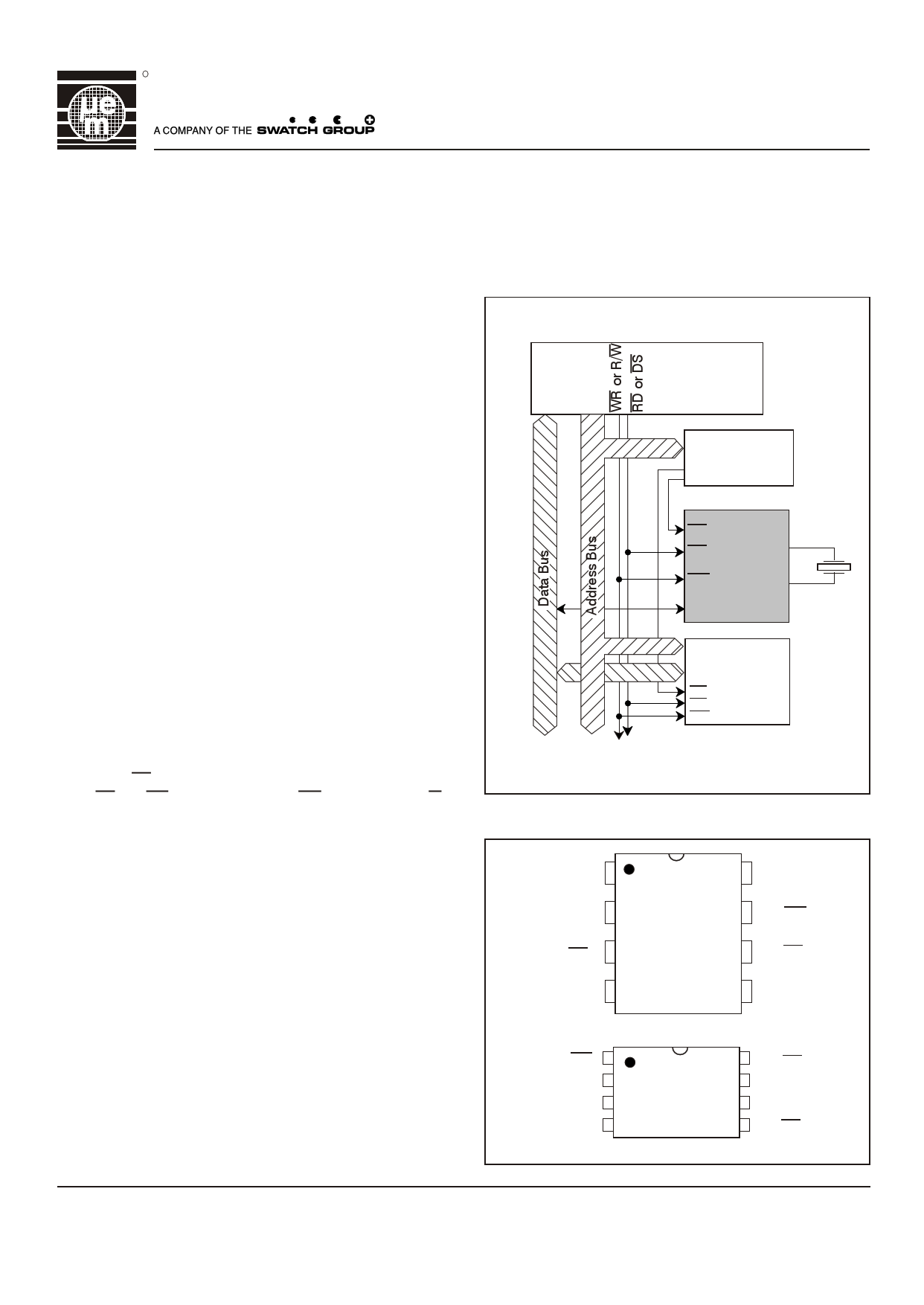
Typical Operating Configuration
CPU
Address
Decoder
CS
RD XI
V3020
WR XO
I/O
RAM
CS
RD
WR
Pin Assignment
S08
XI
XO
V3020
CS
VSS
Fig. 1
VDD
WR
RD
I/O
TSSO8
WR
VDD
XI
XO
V3020
RD
I/O
VSS
CS
Fig. 2
1
1 page 
R
Typical Frequency on I/O Pin
V3020
DF
Fo
[ppm]
+80
Address 10 hex = 00 hex
s/day
+3
Quartz with 8.2 pF load capacitance
+30 +2
-20 +1
-70 0
-120 -1
-170
-50 -30 -10 +10 30
50 70
TA [OC]
Typical drift for ideal 32'768 Hz quartz
90
-2
0 3 6 9 12 15
External trimming capacitor between XO and VSS [pF]
Note : The trimming capacitor value must not exceed 15 pF.
Greater values may disturb the oscillator function.
Fig. 5
Quartz Characteristics
DF
Fo
[ppm]
-100
-200
-300
-400
TO - 100
DF
Fo
=-0.038
ppm
OC2
(T
-
TO)2
±10%
DF/Fo = the ratio of the change in frequency to the nominal value
expressed in ppm (It can be thought of as the frequency
deviation at any temperature.)
T = the temperature of interest in oC
TO = the turnover temperature (25 ± 5 oC)
TO - 50 TO TO+50
Temperature [OC]
TO+100
T [OC]
To determine the clock error (accuracy) at a given temperature, add
the frequency tolerance at 25OC to the value obtained from the
formula above.
Fig. 6
5
5 Page 
R
V3020
Reading the Current Time and Date
Send copy_clock_to_RAM addr. F hex
Read time and data status bits, addr. 1
will indicate which time and date addresses changed since the
last time the command was used (see Fig. 11). The time and
date from the last Copy_clock_to_RAM command is held
unchanged in the RAM, except when power (VDD) has failed
totally. To change the current time and date in the clock, the
desired time and date must first be written to the RAM, the time
set lock bit cleared, and then a Copy_RAM_to_clock command
sent (see Fig. 12). The time set lock bit can be used to prevent
unauthorized setting of the clock.
Setting the Current Time and Date
Is
the seconds
status bit set,
addr. 1,
bit 0
Yes
No
Read seconds, addr. 2
Is
the minutes
status bit set,
addr. 1,
bit 1
Yes
No
Read minutes addr. 3
Similar for hours, day of month,
week day, month, year and
week number
Current time and date
Fig. 11
Clock and Calendar
The Time and date addresses in the RAM (see Table 6) provide
access to the seconds, minutes, hours, day of month, month,
year, week day, and week number. These parameters have the
ranges indicated on Table 6 and are in BCD format. If a
parameter is found to be out of range, it will be cleared on its
being next incremented. The V3020 incorporates leap year
correction and week number calculation. The week number
changes only at the incrementation of the day number from 7 to
1. If week 52 day 7 falls on the 25th, 26th or 27th of December,
then the week number will change to 0 otherwise it will be week
1. Week days are numbered from 1 to 7 with Monday as 1.
Reading of the current time and date must be preceded by a
Copy_clock_to_RAM command. The time and date status bits
Write seconds, minutes, hours, day
of month, week day, month, year
and week number to the RAM
Clear the time set lock bit, addr. 0, bit 4
Send copy_RAM_to_clock command,
addr. E hex
Set the time set lock bit, addr. 0, bit 4
Fig. 12
Frequency Measurement
Setting bit 0 at address 0 will put a pulsed current source (25 mA)
onto the I/O pin, when the device is not chip selected (i.e. CS
input high). The current source will be pulsed on/off at 256 Hz.
The period for ±0 ppm time keeping is 3.90625 ms. To
measure the frequency signal on pin I/O, the data bus must be
high impedance. The best way to ensure this is to hold the
microprocessor and peripherals in reset mode while measuring
the frequency. The clarity of the signal measured at pin I/O will
depend on both the probe input impedance (typically 1 MW)
and the magnitude of the leakage current from other devices
driving the line connected to pin I/O. If the signal measured is
unclear, put a 200 kW resistor from pin I/O to VSS. It should be
noted that the magnitude of the current source (25 mA) is not
sufficient to drive the data bus line in case of any other device
driving the line, but it is sufficient to take the line to a high logic
level when the data bus is in high impedance.
Use a crystal of nominal CL = 8.2 pF as specified in the section
“Operating Conditions”. The MX series from Microcrystal is
recommended. The accuracy of the time keeping is dependent
upon the frequency tolerance and the load capacitance of the
crystal. 11.57 ppm corresponds to one second a day.
11
11 Page | ||
| Páginas | Total 14 Páginas | |
| PDF Descargar | [ Datasheet V30208TSS.PDF ] | |
Hoja de datos destacado
| Número de pieza | Descripción | Fabricantes |
| V30208TSS | Ultra Low Power 1-Bit 32 kHz RTC | ETC |
| Número de pieza | Descripción | Fabricantes |
| SLA6805M | High Voltage 3 phase Motor Driver IC. |
Sanken |
| SDC1742 | 12- and 14-Bit Hybrid Synchro / Resolver-to-Digital Converters. |
Analog Devices |
|
DataSheet.es es una pagina web que funciona como un repositorio de manuales o hoja de datos de muchos de los productos más populares, |
| DataSheet.es | 2020 | Privacy Policy | Contacto | Buscar |