|
|
|
PDF ADF4206 Data sheet ( Hoja de datos )
| Número de pieza | ADF4206 | |
| Descripción | Dual RF PLL Frequency Synthesizers | |
| Fabricantes | Analog Devices | |
| Logotipo | ||
Hay una vista previa y un enlace de descarga de ADF4206 (archivo pdf) en la parte inferior de esta página. Total 24 Páginas | ||
|
No Preview Available !
Dual RF PLL Frequency Synthesizers
ADF4206/ADF4208
FEATURES
ADF4206: 550 MHz/550 MHz
ADF4208: 2.0 GHz/1.1 GHz
2.7 V to 5.5 V power supply
Selectable charge pump supply (VP) allows extended
tuning voltage in 3 V systems
Selectable charge pump currents
On-chip oscillator circuit
Selectable dual modulus prescaler
RF2: 32/33 or 64/65
RF1: 32/33 or 64/65
3-wire serial interface
Power-down mode
APPLICATIONS
Wireless handsets (GSM, PCS, DCS, CDMA, WCDMA)
Base stations for wireless radio (GSM, PCS, DCS,
CDMA, WCDMA)
Wireless LANS
Communications test equipment
CATV equipment
GENERAL DESCRIPTION
The ADF420x family of dual frequency synthesizers are used
to implement local oscillators in the upconversion and down-
conversion sections of wireless receivers and transmitters. Each
synthesizer consists of a low noise, digital, phase frequency detector
(PFD); a precision charge pump; a programmable reference
divider; programmable A and B counters; and a dual modulus
prescaler (P/P + 1). The A (6-bit) and B (11-bit) counters, in
conjunction with the dual modulus prescaler (P/P + 1), implement
an N divider (N = BP + A). In addition, the 14-bit reference
counter (R counter) allows selectable REFIN frequencies at the
PFD input. The on-chip oscillator circuitry allows the reference
input to be derived from crystal oscillators.
A complete phase-locked loop (PLL) can be implemented if the
synthesizers are used with an external loop filter and voltage
controlled oscillators (VCOs).
Control of all the on-chip registers is via a simple 3-wire
interface. The devices operate with a power supply ranging
from 2.7 V to 5.5 V and can be powered down when not in use.
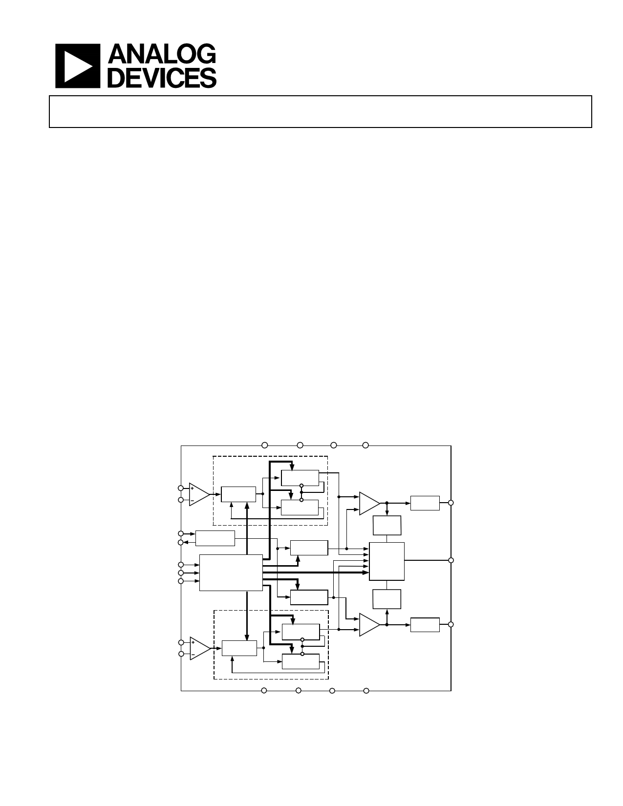
RF2INA
RF2INB
OSCIN
OSCOUT
CLK
DATA
LE
RF1INA
RF1INB
FUNCTIONAL BLOCK DIAGRAM
VDD1
VDD2
VP1
VP2
N = BP + A
RF2
PRESCALER
OSCILLATOR
22-BIT
DATA
REGISTER
SDOUT
N = BP + A
RF1
PRESCALER
11-BIT RF2
B-COUNTER
6-BIT RF2
A-COUNTER
14-BIT RF2
R-COUNTER
14-BIT RF1
R-COUNTER
11-BIT RF1
B-COUNTER
6-BIT RF1
A-COUNTER
ADF4206/ADF4208
PHASE
COMPARATOR
RF2
LOCK
DETECT
CHARGE
PUMP
CPRF2
OUTPUT
MUX
MUXOUT
RF1
LOCK
DETECT
PHASE
COMPARATOR
CHARGE
PUMP
CPRF1
DGNDRF1
AGNDRF1 DGNDRF2
Figure 1.
AGNDRF2
Rev. A
Information furnished by Analog Devices is believed to be accurate and reliable. However, no
responsibility is assumed by Analog Devices for its use, nor for any infringements of patents or other
rights of third parties that may result from its use. Specifications subject to change without notice. No
license is granted by implication or otherwise under any patent or patent rights of Analog Devices.
Trademarksandregisteredtrademarksarethepropertyoftheirrespectiveowners.
One Technology Way, P.O. Box 9106, Norwood, MA 02062-9106, U.S.A.
Tel: 781.329.4700
www.analog.com
Fax: 781.461.3113
©2006 Analog Devices, Inc. All rights reserved.
1 page 
ADF4206/ADF4208
TIMING SPECIFICATIONS
VDD1 = VDD2 = 3 V ± 10%, 5 V ± 10%; VDD1, VDD2 ≤ VP1, VP2 ≤ 6.0 V; AGNDRF1 = DGNDRF1 = AGNDRF2 = DGNDRF2 = 0 V;
TA = TMIN to TMAX, unless otherwise noted; dBm referred to 50 Ω.
Table 2.
Parameter1
t1
t2
t3
t4
t5
t6
Limit at TMIN to TMAX (B Version)
10
10
25
25
10
20
Unit
ns min
ns min
ns min
ns min
ns min
ns min
Test Conditions/Comments
DATA to CLK setup time
DATA to CLK hold time
CLK high duration
CLK low duration
CLK to LE setup time
LE pulse width
1 Guaranteed by design but not production tested.
TIMING DIAGRAM
CLK
DATA DB21 (MSB)
LE
LE
t1 t2
DB20
t3 t4
DB2
DB1
(CONTROL BIT C2)
Figure 2. Timing Diagram
DB0 (LSB)
(CONTROL BIT C1)
t6
t5
Rev. A | Page 5 of 24
5 Page 
CIRCUIT DESCRIPTION
REFERENCE INPUT SECTION
The reference input stage is shown in Figure 22. SW1 and SW2
are normally closed switches. SW3 is normally open. When
power-down is initiated, SW3 is closed and SW1 and SW2 are
opened. Typical recommended external components are shown
in Figure 22.
POWER-DOWN
CONTROL
30pF
30pF
NC 100kΩ
OSCIN NC
SW2
SW1
TO R
COUNTER
BUFFER
OSCOUT
SW3
NO
18kΩ
Figure 22. Reference Input Stage
RF INPUT STAGE
The RF input stage is shown in Figure 23. It is followed by a
2-stage limiting amplifier to generate the CML clock levels
needed for the prescaler.
BIAS
GENERATOR
1.6V
AVDD
2kΩ 2kΩ
RFINA
RFINB
AGND
Figure 23. RF Input Stage
PRESCALER
The dual modulus prescaler (P/P + 1), along with the A and
B counters, enables the large division ratio, N, to be realized
(N = BP + A). This prescaler, operating at CML levels, takes
the clock from the RF input stage and divides it down to a
manageable frequency for the CMOS A and B counters. It is
based on a synchronous 4/5 core.
The prescaler is selectable. Both RF1 and RF2 can be set to
either 32/33 or 64/65. DB20 of the AB counter latch selects the
value. See Figure 29 and Figure 31.
ADF4206/ADF4208
A AND B COUNTERS
The A and B CMOS counters combine with the dual modulus
prescaler to allow a wide ranging division ratio in the PLL
feedback counter. The devices are guaranteed to work when the
prescaler output is 200 MHz or less.
PULSE SWALLOW FUNCTION
The A and B counters, in conjunction with the dual modulus
prescaler, make it possible to generate output frequencies that
are spaced only by the reference frequency divided by R. The
equation for the VCO frequency is
fVCO = [(P × B) + A] × fREFIN/R
where:
fVCO is the output frequency of the external voltage controlled
oscillator (VCO).
P is the preset modulus of the dual modulus prescaler
(32/33, 64/65).
B is the preset divide ratio of the binary 11-bit counter
(2 to 2047).
A is the preset divide ratio of the binary 6-bit A counter
(0 to 63).
fREFIN is the output frequency of the external reference frequency
oscillator.
R is the preset divide ratio of the binary 14-bit programmable
reference counter (1 to 16,383).
R COUNTER
The 14-bit R counter allows the input reference frequency to be
divided down to produce the reference clock to the phase
frequency detector (PFD). Division ratios from 1 to 16,383 are
allowed.
N = BP + A
FROM RF
INPUT STAGE
PRESCALER
P/P + 1
MODULUS
CONTROL
11-BIT B
COUNTER
LOAD
LOAD
6-BIT A
COUNTER
N DIVIDER
Figure 24. A and B Counters
TO PFD
Rev. A | Page 11 of 24
11 Page | ||
| Páginas | Total 24 Páginas | |
| PDF Descargar | [ Datasheet ADF4206.PDF ] | |
Hoja de datos destacado
| Número de pieza | Descripción | Fabricantes |
| ADF4206 | Dual RF PLL Frequency Synthesizers | Analog Devices |
| ADF4207 | Dual RF PLL Frequency Synthesizers | Analog Devices |
| ADF4208 | Dual RF PLL Frequency Synthesizers | Analog Devices |
| Número de pieza | Descripción | Fabricantes |
| SLA6805M | High Voltage 3 phase Motor Driver IC. |
Sanken |
| SDC1742 | 12- and 14-Bit Hybrid Synchro / Resolver-to-Digital Converters. |
Analog Devices |
|
DataSheet.es es una pagina web que funciona como un repositorio de manuales o hoja de datos de muchos de los productos más populares, |
| DataSheet.es | 2020 | Privacy Policy | Contacto | Buscar |