|
|
|
PDF AD7248A Data sheet ( Hoja de datos )
| Número de pieza | AD7248A | |
| Descripción | LC2MOS 12-Bit DACPORTs | |
| Fabricantes | Analog Devices | |
| Logotipo | ||
Hay una vista previa y un enlace de descarga de AD7248A (archivo pdf) en la parte inferior de esta página. Total 16 Páginas | ||
|
No Preview Available !
a
FEATURES
12-Bit CMOS DAC with Output Amplifier and
Reference
Improved AD7245/AD7248:
12 V to 15 V Operation
؎1/2 LSB Linearity Grade
Faster Interface–30 ns typ Data Setup Time
Extended Plastic Temperature Range (–40؇C to +85؇C)
Single or Dual Supply Operation
Low Power–65 mW typ in Single Supply
Parallel Loading Structure: AD7245A
(8+4) Loading Structure: AD7248A
LC2MOS
12-Bit DACPORTs
AD7245A/AD7248A
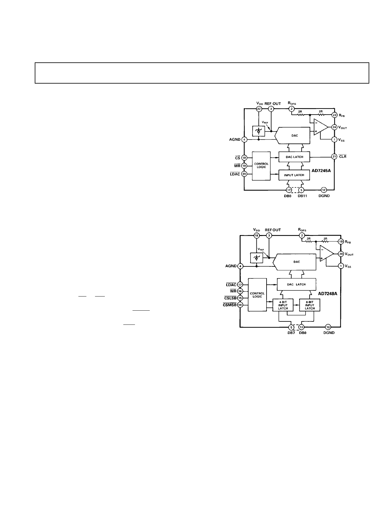
AD7245A FUNCTIONAL BLOCK DIAGRAM
GENERAL DESCRIPTION
The AD7245A/AD7248A is an enhanced version of the industry
standard AD7245/AD7248. Improvements include operation
from 12 V to 15 V supplies, a ± 1/2 LSB linearity grade, faster
interface times and better full scale and reference variations with
VDD. Additional features include extended temperature range
operation for commercial and industrial grades.
The AD7245A/AD7248A is a complete, 12-bit, voltage output,
digital-to-analog converter with output amplifier and Zener volt-
age reference on a monolithic CMOS chip. No external user
trims are required to achieve full specified performance.
Both parts are microprocessor compatible, with high speed data
latches and double-buffered interface logic. The AD7245A ac-
cepts 12-bit parallel data which is loaded into the input latch on
the rising edge of CS or WR. The AD7248A has an 8-bit wide
data bus with data loaded to the input latch in two write opera-
tions. For both parts, an asynchronous LDAC signal transfers
data from the input latch to the DAC latch and updates the ana-
log output. The AD7245A also has a CLR signal on the DAC latch
which allows features such as power-on reset to be implemented.
The on-chip 5 V buried Zener diode provides a low noise, tem-
perature compensated reference for the DAC. For single supply
operation, two output ranges of 0 V to +5 V and 0 V to +10 V
are available, while these two ranges plus an additional ± 5 V
range are available with dual supplies. The output amplifiers are
capable of developing +10 V across a 2 kΩ load to GND.
The AD7245A/AD7248A is fabricated in linear compatible
CMOS (LC2MOS), an advanced, mixed technology process that
combines precision bipolar circuits with low power CMOS logic.
The AD7245A is available in a small, 0.3" wide, 24-pin DIP and
DACPORT is a registered trademark of Analog Devices, Inc.
AD7248A FUNCTIONAL BLOCK DIAGRAM
SOIC and in 28-terminal surface mount packages. The
AD7248A is packaged in a small, 0.3" wide, 20-pin DIP and
SOIC and in 20-terminal surface mount packages.
PRODUCT HIGHLIGHTS
1. The AD7245A/AD7248A is a 12-bit DACPORT® on a single
chip. This single chip design and small package size offer
considerable space saving and increased reliability over
multichip designs.
2. The improved interface times on the part allows easy, direct
interfacing to most modern microprocessors.
3. The AD7245A/AD7248A features a wide power supply range
allowing operation from 12 V supplies.
REV. A
Information furnished by Analog Devices is believed to be accurate and
reliable. However, no responsibility is assumed by Analog Devices for its
use, nor for any infringements of patents or other rights of third parties
which may result from its use. No license is granted by implication or
otherwise under any patent or patent rights of Analog Devices.
One Technology Way, P.O. Box 9106, Norwood, MA 02062-9106, U.S.A.
Tel: 617/329-4700
Fax: 617/326-8703
1 page 
AD7245A/AD7248A
AD7248A PIN FUNCTION DESCRIPTION
(DIP PIN NUMBERS)
Pin Mnemonic Description
l VSS
Negative Supply Voltage (0 V for single
supply operation).
2 ROFS
Bipolar Offset Resistor. This provides
access to the on-chip application resistors
and allows different output voltage ranges.
3 REF OUT Reference Output. The on-chip reference
is provided at this pin and is used when
configuring the part for bipolar outputs.
4 AGND
Analog Ground.
5 DB11
Data Bit 11. Most Significant Bit (MSB).
6-11 DB10-DB5 Data Bit 10 to Data Bit 5.
12 DGND
Digital Ground.
13-16 DB4-DB1 Data Bit 4 to Data Bit 1.
17 DB0
Data Bit 0. Least Significant Bit (LSB).
18 CS
Chip Select Input (Active LOW). The de-
vice is selected when this input is active.
Pin Mnemonic Description
19 WR
Write Input (Active LOW). This is used in
conjunction with CS to write data into the
input latch of the AD7245A.
20 LDAC
Load DAC Input (Active LOW). This is
an asynchronous input which when active
transfers data from the input latch to the
DAC latch.
21 CLR
Clear Input (Active LOW). When this in-
put is active the contents of the DAC latch
are reset to all 0s.
22 VDD
23 RFB
Positive Supply Voltage.
Feedback Resistor. This allows access to
the amplifier’s feedback loop.
24 VOUT
Output Voltage. Three different output
voltage ranges can be chosen: 0 V to +5 V,
0 V to +10 V or –5 V to +5 V.
DIP and SOIC
AD7245A PIN CONFIGURATIONS
LCCC
PLCC
REV. A
–5–
5 Page 
AD7245A/AD7248A
BIPOLAR CONFIGURATION
The bipolar configuration for the AD7245A/AD7248A, which
gives an output voltage range from –5 V to +5 V, is achieved by
connecting the ROFS input to REF OUT and connecting RFB
and VOUT. The AD7245A/AD7248A must be operated from
dual supplies to achieve this output voltage range. The code
table for bipolar operation is shown in Table IV.
Table IV. Bipolar Code Table
DAC Latch Contents
MSB
LSB
Analog Output, VOUT
1111 1111
2047
1 1 1 1 +VREF × 2048
1000 0000
1000 0000
0111 1111
0001
0000
1111
1
+VREF × 2048
0V
1
–VREF × 2048
0000 0000
2047
0 0 0 1 –VREF × 2048
0000 0000
0000
–VREF ×
2048
2048
=
– VREF
NOTE:
1
LSB
=
2
×
VREF(2–11)
=
VREF
1
2048
AGND BIAS
The AD7245A/AD7248A AGND pin can be biased above sys-
tem GND (AD7245A/AD7248A DGND) to provide an offset
“zero” analog output voltage level. With unity gain on the am-
plifier (ROFS = VOUT = RFB) the output voltage, VOUT is ex-
pressed as:
VOUT = VBIAS + D ؋ VREF
where D is a fractional representation of the digital word in the
DAC latch and VBIAS is the voltage applied to the AD7245A/
AD7248A AGND pin.
Because the current flowing out of the AGND pin varies with
digital code, the AGND pin should be driven from a low imped-
ance source. A circuit configuration is outlined for AGND bias
in Figure 9 using the AD589, a +1.23 V bandgap reference.
If a gain of 2 is used on the buffer amplifier the output voltage,
VOUT is expressed as
VOUT = 2(VBIAS + D ؋ VREF)
In this case care must be taken to ensure that the maximum out-
put voltage is not greater than VDD –3 V. The VDD–VOUT over-
head must be greater than 3 V to ensure correct operation of the
part. Note that VDD and VSS for the AD7245A/AD7248A must
be referenced to DGND (system GND). The entire circuit can
be operated in single supply with the VSS pin of the AD7245A/
AD7248A connected to system GND.
Figure 9. AGND Bias Circuit
PROGRAMMABLE CURRENT SINK
Figure 10 shows how the AD7245A/AD7248A can be config-
ured with a power MOSFET transistor, the VN0300M, to pro-
vide a programmable current sink from VDD or VSOURCE. The
VN0300M is placed in the feedback of the AD7245A/
AD7248A amplifier. The entire circuit can be operated in single
supply by tying the VSS of the AD7245A/AD7248A to AGND.
The sink current, ISINK, can be expressed as:
ISINK =
D × VREF
R1
Figure 10. Programmable Current Sink
Using the VN0300M, the voltage drop across the load can typi-
cally be as large as VSOURCE –6 V) with VOUT of the DAC at
+5 V. Therefore, for a current of 50 mA flowing in the R1 (with
all 1s in the DAC register) the maximum load is 200 Ω with
VSOURCE = +15 V. The VN0300M can actually handle currents
up to 500 mA and still function correctly in the circuit, but in
practice the circuit must be used with larger values of VSOURCE
otherwise it requires a very small load.
Since the tolerance value on the reference voltage of the
AD7245A/AD7248A is ± 0.2%, then the absolute value of ISINK
can vary by ± 0.2% from device to device for a fixed value of R1.
Because the input bias current of the AD7245A/AD7248A’s op
amp is only of the order of picoamps, its effect on the sink cur-
rent is negligible. Tying the ROFS input to RFB input reduces this
effect even further and prevents noise pickup which could occur
if the ROFS pin was left unconnected.
REV. A
–11–
11 Page | ||
| Páginas | Total 16 Páginas | |
| PDF Descargar | [ Datasheet AD7248A.PDF ] | |
Hoja de datos destacado
| Número de pieza | Descripción | Fabricantes |
| AD7248 | LC2MOS 12-Bit DACPORT | Analog Devices |
| AD7248A | LC2MOS 12-Bit DACPORTs | Analog Devices |
| Número de pieza | Descripción | Fabricantes |
| SLA6805M | High Voltage 3 phase Motor Driver IC. |
Sanken |
| SDC1742 | 12- and 14-Bit Hybrid Synchro / Resolver-to-Digital Converters. |
Analog Devices |
|
DataSheet.es es una pagina web que funciona como un repositorio de manuales o hoja de datos de muchos de los productos más populares, |
| DataSheet.es | 2020 | Privacy Policy | Contacto | Buscar |