|
|
|
PDF AD633 Data sheet ( Hoja de datos )
| Número de pieza | AD633 | |
| Descripción | Low Cost Analog Multiplier | |
| Fabricantes | Analog Devices | |
| Logotipo | ||
Hay una vista previa y un enlace de descarga de AD633 (archivo pdf) en la parte inferior de esta página. Total 20 Páginas | ||
|
No Preview Available !
Data Sheet
FEATURES
4-quadrant multiplication
Low cost, 8-lead SOIC and PDIP packages
Complete—no external components required
Laser-trimmed accuracy and stability
Total error within 2% of full scale
Differential high impedance X and Y inputs
High impedance unity-gain summing input
Laser-trimmed 10 V scaling reference
APPLICATIONS
Multiplication, division, squaring
Modulation/demodulation, phase detection
Voltage-controlled amplifiers/attenuators/filters
GENERAL DESCRIPTION
The AD633 is a functionally complete, four-quadrant, analog
multiplier. It includes high impedance, differential X and Y inputs,
and a high impedance summing input (Z). The low impedance
output voltage is a nominal 10 V full scale provided by a buried
Zener. The AD633 is the first product to offer these features in
modestly priced 8-lead PDIP and SOIC packages.
The AD633 is laser calibrated to a guaranteed total accuracy of
2% of full scale. Nonlinearity for the Y input is typically less
than 0.1% and noise referred to the output is typically less than
100 µV rms in a 10 Hz to 10 kHz bandwidth. A 1 MHz bandwidth,
20 V/µs slew rate, and the ability to drive capacitive loads make
the AD633 useful in a wide variety of applications where
simplicity and cost are key concerns.
The versatility of the AD633 is not compromised by its simplicity.
The Z input provides access to the output buffer amplifier, enabling
the user to sum the outputs of two or more multipliers, increase
the multiplier gain, convert the output voltage to a current, and
configure a variety of applications. For further information, see
the Multiplier Application Guide.
Low Cost
Analog Multiplier
AD633
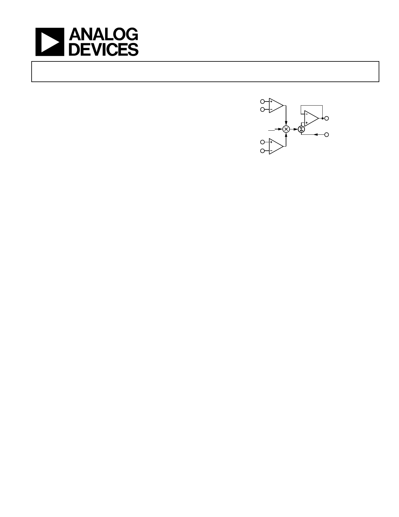
FUNCTIONAL BLOCK DIAGRAM
X1
1
X2
AW
1
10V
Y1
1
Y2
Z
Figure 1.
The AD633 is available in 8-lead PDIP and SOIC packages. It is
specified to operate over the 0°C to 70°C commercial temperature
range (J Grade) or the −40°C to +85°C industrial temperature
range (A Grade).
PRODUCT HIGHLIGHTS
1. The AD633 is a complete four-quadrant multiplier offered
in low cost 8-lead SOIC and PDIP packages. The result is a
product that is cost effective and easy to apply.
2. No external components or expensive user calibration are
required to apply the AD633.
3. Monolithic construction and laser calibration make the
device stable and reliable.
4. High (10 MΩ) input resistances make signal source
loading negligible.
5. Power supply voltages can range from ±8 V to ±18 V. The
internal scaling voltage is generated by a stable Zener diode;
multiplier accuracy is essentially supply insensitive.
Rev. K
Document Feedback
Information furnished by Analog Devices is believed to be accurate and reliable. However, no
responsibilityisassumedbyAnalogDevices for itsuse,nor foranyinfringementsofpatentsor other
rights of third parties that may result from its use. Specifications subject to change without notice. No
license is granted by implication or otherwise under any patent or patent rights of Analog Devices.
Trademarksandregisteredtrademarksarethepropertyoftheirrespectiveowners.
One Technology Way, P.O. Box 9106, Norwood, MA 02062-9106, U.S.A.
Tel: 781.329.4700
©2015 Analog Devices, Inc. All rights reserved.
Technical Support
www.analog.com
1 page 
Data Sheet
AD633
PIN CONFIGURATIONS AND FUNCTION DESCRIPTIONS
X1 1
1
X2 2
Y1 3
1
10V
A
Y2 4
1
AD633JN/AD633AN
W = (X1 – X2)(Y1 – Y2) + Z
10V
8 +VS
7W
6Z
5 –VS
Figure 2. 8-Lead PDIP
Y1 1
1
1
Y2 2
1
10V
–VS 3
A
Z4
AD633JR/AD633AR
W = (X1 – X2)(Y1 – Y2) + Z
10V
8 X2
7 X1
6 +VS
5W
Figure 3. 8-Lead SOIC
Table 4. 8-Lead PDIP Pin Function Descriptions
Pin No. Mnemonic Description
1 X1
X Multiplicand Noninverting Input
2 X2
X Multiplicand Inverting Input
3 Y1
Y Multiplicand Noninverting Input
4 Y2
Y Multiplicand Inverting Input
5 −VS
Negative Supply Rail
6Z
Summing Input
7W
Product Output
8 +VS
Positive Supply Rail
Table 5. 8-Lead SOIC Pin Function Descriptions
Pin No. Mnemonic Description
1 Y1 Y Multiplicand Noninverting Input
2 Y2 Y Multiplicand Inverting Input
3 −VS Negative Supply Rail
4Z
Summing Input
5 W Product Output
6 +VS Positive Supply Rail
7 X1 X Multiplicand Noninverting Input
8 X2 X Multiplicand Inverting Input
Rev. K | Page 5 of 20
5 Page 
Data Sheet
AD633
For example, if R = 8 kΩ and C = 0.002 μF, then Output A has a
pole at frequencies from 100 Hz to 10 kHz for EC ranging from
100 mV to 10 V. Output B has an additional 0 at 10 kHz (and
can be loaded because it is the low impedance output of the
multiplier). The circuit can be changed to a high-pass filter Z
interchanging the resistor and capacitor as shown in Figure 21.
CONTROL
INPUT EC
SIGNAL
INPUT ES
1 X1
dB
+15V
0
+VS 8
0.1µF
f1 f2
f
OUTPUT B
+6dB/OCTAVE
OUTPUT A
2 X2
W7
AD633JN
3 Y1
Z6
4 Y2
–VS 5
0.1µF
OUTPUT B
C
OUTPUT A
R
–15V
Figure 21. Voltage-Controlled, High-Pass Filter
VOLTAGE-CONTROLLED QUADRATURE OSCILLATOR
Figure 22 shows two multipliers being used to form integrators
with controllable time constants in second-order differential
equation feedback loop. R2 and R5 provide controlled current
output operation. The currents are integrated in capacitors C1
and C2, and the resulting voltages at high impedance are applied
to the X inputs of the next AD633. The frequency control input, EC,
connected to the Y inputs, varies the integrator gains with a
calibration of 100 Hz/V. The accuracy is limited by the Y input
offsets. The practical tuning range of this circuit is 100:1. C2
(proportional to C1 and C3), R3, and R4 provide regenerative
feedback to start and maintain oscillation. The diode bridge, D1
through D4 (1N914s), and Zener diode D5 provide economical
temperature stabilization and amplitude stabilization at ±8.5 V
by degenerative damping. The output from the second integrator
(10 V sin ωt) has the lowest distortion.
AUTOMATIC GAIN CONTROL (AGC) AMPLIFIERS
Figure 23 shows an AGC circuit that uses an rms-to-dc
converter to measure the amplitude of the output waveform.
The AD633 and A1, half of an AD712 dual op amp, form a
voltage-controlled amplifier. The rms-to-dc converter,
an AD736, measures the rms value of the output signal. Its
output drives A2, an integrator/comparator whose output
controls the gain of the voltage-controlled amplifier. The
1N4148 diode prevents the output of A2 from going negative.
R8, a 50 kΩ variable resistor, sets the output level of the circuit.
Feedback around the loop forces the voltages at the inverting
and noninverting inputs of A2 to be equal, thus the AGC.
D5
1N5236
D1
1N914
D3
1N914
D2
1N914
R1
1kΩ
EC
D4
1N914
+15V
1 X1
+VS 8
0.1µF
2 X2
W7
AD633JN
3 Y1
Z6
4 Y2
–VS 5
0.1µF
–15V
R2
16kΩ
C1
0.01µF
+15V
1 X1
+VS 8
0.1µF
2 X2
W7
AD633JN
3 Y1
Z6
4 Y2
–VS 5
0.1µF
–15V
Figure 22. Voltage-Controlled Quadrature Oscillator
(10V) cos ωt
C2
0.01µF
R4
16kΩ
R3
330kΩ
(10V) sin ωt
R5
16kΩ
C3
0.01µF
f = EC = kHz
10V
Rev. K | Page 11 of 20
11 Page | ||
| Páginas | Total 20 Páginas | |
| PDF Descargar | [ Datasheet AD633.PDF ] | |
Hoja de datos destacado
| Número de pieza | Descripción | Fabricantes |
| AD630 | Balanced Modulator/Demodulator | Analog Devices |
| AD6311 | 1/8- to 1/16 Duty VFD Controller/Driver | Anachip |
| AD6312 | 1/4- to 1/11 Duty VFD Controller/Driver | Anachip |
| AD6315 | 1/4- to 1/12 Duty VFD Controller/Driver | Anachip |
| Número de pieza | Descripción | Fabricantes |
| SLA6805M | High Voltage 3 phase Motor Driver IC. |
Sanken |
| SDC1742 | 12- and 14-Bit Hybrid Synchro / Resolver-to-Digital Converters. |
Analog Devices |
|
DataSheet.es es una pagina web que funciona como un repositorio de manuales o hoja de datos de muchos de los productos más populares, |
| DataSheet.es | 2020 | Privacy Policy | Contacto | Buscar |